Laser direct writing builds biostructures
Douglas Chrisey, Alberto Piqué, Jim Fitz-Gerald, Bradley Ringeisen, and Rohit Mohdi
A pulsed UV laser writes thin-film CAD patterns and arrays of high-quality crystalline materials on delicate substrates, including the abdomen of a honeybee.
In the electronics industry, the trend toward miniaturization of both components and subsystems has largely overlooked mesoscale passive devices (~10 µm to 1 mm in size), mostly because of difficulties with their fabrication and performance. This is changing as the continuous drive for new electronic and sensor devices pushes current technologies to their limits. New processes are required to increase the density and reduce the size of mesoscale passive devices, while at the same time simplifying their manufacturing and accelerating their prototyping times.
Buoyed by recent developments in materials and laser-based materials processing, the Naval Research Laboratory (NRL; Washington, DC) has developed a laser-based direct-write techniquematrix-assisted pulsed-laser-evaporation direct write (MAPLE DW)to simplify the fabrication of high-quality mesoscale electronic components and biostructures and reduce processing costs.1,2 This technique, which will be commercialized by NRL industrial-partner Potomac Photonics (Lanham, MD), has possible applications ranging from electroluminescent displays to the direct writing of biomaterials for tissue engineering and array-based biosensors.
Direct-write process
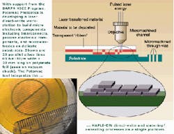
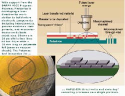
To build mesoscale patterns and arrays on even the most delicate structures, engineers combine a standard laser-writing techniquelaser-induced forward transferwith the vacuum-based MAPLE process.3,4 Material deposition begins when the beam of a high-repetition-rate, 355-nm ultraviolet (UV) laser is focused through a transparent support onto a 1- to 10-µm matrix-based coating on its opposite side (see figure above). The coating transfers to the receiving substrate and, with some thermal processing, forms an adherent film with electronic properties comparable to devices fabricated by typical thick-film approaches such as screen printing. The transparent support and coating are jointly referred to as a ribbon in an analogy to a conventional typewriter.
The technique forms electronic circuit patterns with feature resolution smaller than 10 µm by synchronously moving the ribbon to a fresh, unexposed region and then moving the receiving substrate approximately one beam diameter. The resulting individual mesoscopic bricks of electronic material, one per laser shot, are then assembled into the desired pattern. A rapid ribbon change from a metal to a dielectric and back to a metal allows building parallel-plate capacitors or other three-dimensional (3-D) structures. When the ribbon is removed, the MAPLE DW system has all the attributes of a laser micromachining system. Thus, engineers can etch grooves or vias in the substrate, preclean the surface, or even surface anneal or etch individual components to improve their performance or dimensional accuracy.
There are many different ways to direct write or transfer patterned materials including plasma-spray, laser-particle guidance, micropen, ink jet, e-beam, focused ion beam, and several liquid or droplet microdispensing approaches.5,6 These techniques require high-quality starting materials, including powders, nanopowders, flakes, modified surface coatings and properties, organic precursors, binders, solvents, dispersants, and surfactants.7,8 These diverse materials, which have often been developed specifically for processing temperatures below 300°C to 400°C, will allow fabrication of passive electronic components and RF devices that offer the performance of conventional thick-film materials on low-temperature flexible substrates such as plastics, paper, and fabrics.
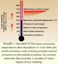
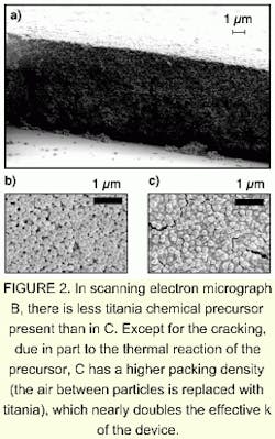
Fabricating high-quality crystalline materials at temperatures below 400°C is nearly impossible, though (see Fig. 1). Just by combining spherical powders with a narrow size distribution, the highest possible packing density is ~74% for the face-centered cubic structure. This 26% air matrix reduces the effective dielectric constant of an insulator by almost an order of magnitude, highlighting the importance of reducing the porosity in transferred materials. Particle-to-particle bonding is even more difficult at low temperatures. One alternative is to use a high-density packed powder of varying particle sizes combined with chemical precursors that form low-melting-point nanoparticles in situ to chemically fuse the powder. A key step in the MAPLE DW process is thus to optimize the relative ratios of powders, nanoparticles, and chemical precursors to produce good uniformity and dense packing (see Fig. 2).
To further improve the electronic properties for low-temperature processing, especially of the oxide ceramics, engineers use laser sintering to enhance particle-to-particle bonding and reduce porosity. For infrared (IR) laser wavelengths (1 to 10 µm), the penetration depth for different materials is on the order of microns, allowing the benefits of higher-temperature processing on thermally sensitive substrates. Ultimately, laser annealing should come close to allowing reacted precursors on biological substrates and some level of bulk diffusion on polyimide substrates.
From art to part fast
Working from a CAD software file, the MAPLE DW process can produce a variety of passive electronic devices, including simple interconnects with resistivity close to two times that of bulk silver and phosphor arrays for displays (see Laser Focus World, May 2000, p. 20). Other possibilities include nichrome coplanar resistors or polymer thick-film resistors whose resistance can be accurately predicted over five decades, capacitors with dielectric constants between 4 and 100 and low losses (<1%), and 3-D multiturn yttrium iron garnet core inductors. Benefits of such mesoscopic conformal passive electronics include reduced size and weight, improved performance and robustness, and rapid prototyping for circuit modeling, design, and testing.
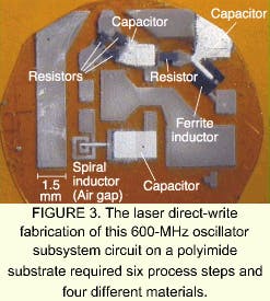
The state of the art for write speed is 200 mm/s, so engineers can go from a concept to a working prototype in a very short time. Equally important is the capability to work with multiple materials in a single CAD file to represent a sophisticated electronic subsystem. One example is a 600-MHz oscillator designed, modeled, fabricated and tested at the NRL on a flexible polyimide substrate using four different electronic materials (see Fig. 3).
On bees and beyond
Currently, the process of direct-writing electronic materials on living biological substrates or specimens remains relatively unexplored territory. There is, however, a need not only to electrically interface to the animal kingdom to better understand it, but also to manipulate it. One example is to train and use adult worker honeybees (Apis Mellifera) to detect extremely low levels of dangerous chemicals (unexploded ordinance, environmental toxins, for example). To locate the chemicals over the several square kilometers that the bee typically covers and not perturb the flight of the workers, scientists must attach an extremely small antenna to each animala so-far-unsuccessful process that involved gluing antennae to the bees.
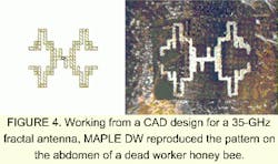
With the MAPLE DW technique, it is possible to reduce the size of the antenna to its fundamental electromagnetic limit. An example is a fractal-reflecting antenna with features representing approximately 1 mm on edge that has been successfully written onto the abdomen of a dead honeybee (see Fig. 4). Fractal antennas are interesting in this application because the pseudorandom bends reduce the size and weight while providing multiband capability. NRL researchers have demonstrated a similar-size coating on an anesthetized bee with no apparent harm.
Advances in the research community's understanding of new materials and laser-material interaction have driven the progress seen in the direct writing of electronic materials, but the recent advances in the direct writing of biomaterials has been driven by advances in the UV-laser-based transfer technology. MAPLE DW in particular can be an extremely gentle transfer process. At the NRL, using ribbons made of an aqueous composite mixture, scientists have transferred patterns of viable E. coli onto various substrates.
Micron-scale patterns of viable cells and the methods to manufacture them are required for next-generation tissue engineering, fabrication of cell-based microfluidic biosensor arrays, and selective separation and culturing of microorganisms. There is no current technology capable of instantaneously writing adjacent patterns of different viable cells from a multi-cellular ribbon or palette. With the NRL laser direct-write technique, it may someday be possible to create 3-D mesoscopically engineered structures of living cells, proteins, DNA strands, and antibodies. In line with this, it may become beneficial to fabricate electronic devices on the same substrate to rapidly generate cell-based biosensors and bioelectronic interfaces to probe, among other things, intercellular signaling.
MAPLE DW represents a paradigm shift for conventional electronic manufacturing and prototyping processes. The ability to generate components on demand any place on any substrate in a matter of minutes, instead of weeks, will provide engineers with a unique opportunity to bring new designs to life that are infeasible with today's manufacturing techniques.
ACKNOWLEDGMENTS
The authors would like to acknowledge support for this work from the Office of Naval Research and the MICE Program in the Defense Advanced Projects Research Agency, as well as the research efforts of R. C. Auyeung, H. D. Wu, R. Chung, B. H. Thompson, D. Young, and D. Weir.
REFERENCES
- D. B. Chrisey et al., Appl. Surf. Sci. 154-155, 593 (2000).
- J. M. Fitz-Gerald et al., Appl. Phys. Lett. 76, 1386 (2000).
- I. Zergioti et al., Appl. Phys. A 66, 579 (1998).
- A. Pique et al., Proc. MRS 526, 421 (1998).
- M. J. Renn, R. Pastel, and H. J. Lewandowski, Phys. Rev. Lett. 82, 1574 (1999).
- P. Blazdell and S. Kurdoda, Surf. Coat. Tech. 123, 239 (2000).
- B. H. King, D. Dimos, P. Yang, and S. L. Morissette, J. Electroceramics 3, 173 (1999).
- B. R. Ringeisen et al., unpublished results.
DOUGLAS CHRISEY is a supervisory research physicist, ALBERTO PIQUÉ is a material scientist, JIM FITZ-GERALD is an ASEE postdoctoral associate, and BRADLEY RINGEISEN is a postdoctoral research associate with the Naval Research Laboratory, Washington, DC 20375. ROHIT MOHDI is a graduate student at George Washington University; e-mail: [email protected].
