FLAT-PANEL DISPLAYS: Solid-state emitter may cut costs of FEDs
Researchers at the University of Lyon (Villerubanne, France) and the University of Franche-Comté (Bescançon, France) have developed a computational model to explain their previously reported success in reducing the field strength required to remove an electron from a metal surface by two orders of magnitude.1 The method and the explanation offer exciting possibilities for overcoming two of the primary technological barriers to achieving market-competitive production costs of field-emission displays (FEDs) for flat-panel computer monitors.
Currently, FED devices require a very strong electric field to transfer electrons from a dense two-dimensional array of sharp and precisely uniform needle-tipped electrodes across a vacuum and to a screen where the electrons actually produce illumination. The high-voltage circuitry needed to provide the strong electric field and the need for precise uniformity over literally millions of needle-shaped electrodes are primary contributors to the high cost of FEDs.
During the meeting of the Materials Research Society last Spring in San Francisco, CA, the French research team reported that they had found ways around both of these problems by depositing an ultrathin semiconductor (UTSC) layer on top of a metallic (platinum sheet) to create a solid-state, field-controlled electron emitter (SSE). Conventional electron emission systems require either temperatures in excess of 1300 K or electric-field strengths in excess of 5000 V/µm to obtain threshold emission current. The electric-field strength threshold for SSE emission, however, was on the order of 50 V/µm at about 300 K in a vacuum of only 10-7 Torr. The UTSC of the SSE cathode consisted of a 5-nm-thick, wide-bandgap, n-type semiconductor (titanium oxide). In addition to lowering the electric-field threshold by two orders of magnitude, the SSE provided uniform electron emission from its surface, eliminating the requirement in conventional systems for large-scale, precision fabrication of complex cathode structures.
Mathematical model
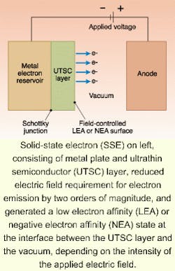
Since initially observing the effect, the researchers have developed a qualitative two-step, mathematical model that appears to explain the apparent lowering of the cathode surface barrier to about 0.1 eV after SSE fabrication and application of an electric field. In the first step of the model, electrons from the platinum plate enter the Schottky junction in the SSE between the metal and the UTSC layer (see Figure). In the second step, the injected electrons induce a large band bending in the UTSC layer that drastically lowers the emission barrier between the SSE cathode and the vacuum.
Based on a numerical integration of Poisson's equation, the researchers theorized that space-charge accumulation in the conduction band of the UTSC layer began at approximately 50 V/µm and was initially driven (in the first step of the model) to a relatively small equilibrium level of space charge based on the strength of the applied electric field. In the second step, the equilibrium level of space charge grew large enough due to electron injection through thermionic processes and tunneling to produce significant band bending in the UTSC layer and a low electron affinity at the vacuum surface. In this second equilibrium condition, further increases in applied electric field had little effect on the equilibrium charge distribution in the UTSC layer, but tended to lower the barrier between the UTSC layer and the vacuum. As the applied voltage is increased, however, the vacuum-UTSC barrier eventually develops a negative electron affinity leading to an "explosive increase" in current density.
The researchers also found that the equilibrium level of space charge in the UTSC conduction band varied with the inverse of the UTSC thickness and was related to the ability to reach an equilibrium level within the available space. Increasing the thickness to 6 or 7 nm prevented the lowering of emission barriers to states of low electron affinity, and decreasing the thickness to about 4 nm allowed the space charge distribution to extend beyond the UTSC layer conduction band, which also prevented significant band bending.
One of the researchers, Vu Thien Binh, has begun to develop the research findings into a product with hopes of achieving commercial availability within two years.
REFERENCE
- V. T. Binh and C. Adessi, PRL 85(4), 864 (July, 24, 2000).
About the Author
Hassaun A. Jones-Bey
Senior Editor and Freelance Writer
Hassaun A. Jones-Bey was a senior editor and then freelance writer for Laser Focus World.
