Organic light-emitting diodes (OLEDs) show considerable promise for near-to-the-eye virtual display applications, mostly because their emissive behavior promotes wide-angle viewing, even in bright environments. Processing during fabrication also is at low temperatures—a key requirement of flat-panel displays. Practicality is further enhanced if the devices can be integrated with complementary metal-oxide-silicon (CMOS) circuitry to allow high quantum efficiency with a low operating voltage and simple processing steps. Perhaps the last requirement on any display researcher's wish list would be for an active matrix approach, which is highly desirable for high-definition displays that require many pixels to be addressed at video rates.
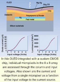
Such displays now may be one step closer to reality if research under way at the Optical Sciences Center of the University of Arizona (Tucson, AZ) is any indication. Center researchers recently demonstrated an 8 x 8 array of 90-µm pixels based on OLEDs heterogeneously integrated with foundry-supplied CMOS circuitry. The resulting active matrix configuration allowed individual pixels to be driven by a current source while providing light output easily viewable with the naked eye. Luminance measurements indicated a maximum luminance of 7012 cd/m2 with a CMOS input voltage of 5V.
The center's initial array design included a 55-µm separation between the square pixels, each of which had its own LED pixel driver to make the circuitry active-matrix addressable.1 The circuit design was based on a modified current mirror that allowed the input voltage to control the current through the OLED. In other words, the voltage across the device adjusted itself to allow the desired current through the OLED up to the limits of the compliance voltage, which was designed to be greater than 10 V for this circuit.
Tests of the drive circuitry indicated that a compliance voltage of 11.1 V is obtainable for the OLED driver with a current level of 55 µA. The individual OLED of the 8 x 8 array was addressed using a control line that supplied a voltage to the gate of all of a row of control transistors. Each pixel was then controlled using the bias on the drain of the control transistor.
In the initial OLED-CMOS integration, OLEDS were based on an emitting layer of tris-(8-hydroxyquinoline)aluminum (Alq3) doped with coumarin 6 to provide green light emission (see figure). A layer of N,N'-diphenyl-N, N'-bis(3-methylphenyl)1-1'-biphenyl 1-4,4'-diamine (TPD) was used as a hole transport layer. The buffer layer between the TPD and the CMOS anode metal was poly(ethylenedioxythiophene) doped with polystyrenesulfonate. With each micropixel driven by an individual current source, the device emitted bright light through a semitransparent magnesium-silver cathode.
According to center researchers, the effort to integrate OLEDs with CMOS circuitry took advantage of conventional CMOS semiconductor processing steps whenever possible. To prove scalability of the technique to the full wafer level, the scientists used a 2-in. silicon wafer to make two-dimensional displays that covered the entire wafer. The fabrication process involved spin casting of polymeric materials onto custom-designed CMOS circuitry, followed by the vacuum deposition of transport and emissive organic layers.
REFERENCE
- D. L. Mathine et al., App. Phys. Lett. 76, 3849 (June 26, 2000).
About the Author
Paula Noaker Powell
Senior Editor, Laser Focus World
Paula Noaker Powell was a senior editor for Laser Focus World.
