The advent of hybrid optoelectronic devices that include thousands or millions of discrete elements poses a problem—how to make such devices in large quantities and at low cost. One time-consuming (and therefore expensive) step is placing each element in its proper position. With the advent of large-scale pick-and-place methods, potential applications such as displays that contain closely packed light-emitting-diode (LED) chips as emitters may become economical. Researchers at the University of California at San Diego (UCSD) have developed a fluidic processing method that moves optoelectronic devices or other small objects by electrical or optical addressing and shows potential for massively parallel use.
The objects to be positioned are immersed between two plates in an electrolytic solution, with one of the plates being the silicon substrate onto which the devices would eventually be fixed. The top glass plate is coated with a transparent indium tin oxide electrode; an electric field perpendicular to the substrate exerts a force on the objects, reducing friction. Electrical addressing is the method of choice for positioning large numbers of identical devices but requires prepatterning of the substrate, say the researchers. Optical addressing eliminates prepatterning and also allows continuous motion for the highest positioning accuracy.
In electrical addressing, 100-µm-diameter circular openings in a silicon nitride coating on the n-type silicon substrate attract negatively charged objects (for test purposes, polystyrene beads) to the openings under a positive bias voltage. Subsequent reversal of the voltage disperses the beads in a desired random distribution. The process worked for beads ranging from 0.8 to 20 µm in diameter.
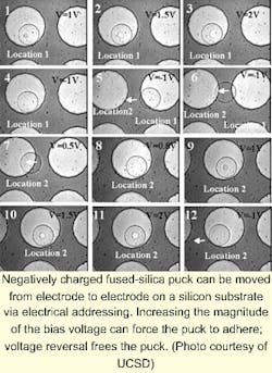
The researchers tried larger objects, fabricating 50-µm-diameter fused-silica pucks that were negatively charged by immersing them in a sodium dodecyl sulfate and water solution and then rinsing them. Applying a bias voltage attracted a puck to an electrode; increasing the voltage pulled the puck against the substrate, causing it to adhere (see figure). Interference fringes show where the puck adheres. Reversing the voltage causes the adhesion to disappear. Proper switching of voltages enabled the researchers to move the puck from one electrode to the next in discrete steps all the way to the end of the electrochemical cell. Finally, the researchers placed three 50-µm-diameter LEDs using electrical addressing, positioning the devices concurrently (only three LEDs were available for test).
Optical addressing
Optical addressing requires the use of a photosensitive substrate. An external mask illuminates a specific place on the substrate. Areas of light on the substrate form a Schottky diode at the substrate surface, forming highly charged localized regions to which oppositely charged particles are attracted. In a demonstration of optical addressing, 0.87-µm-diameter polystyrene beads immersed in deionized water were moved using 632-nm light from a helium-neon laser. In combination with a mask containing either a circular or elliptical transmissive hole, the beads squeezed themselves into an area corresponding to the projected hole image. Optical addressing has been used to position objects up to 10 µm in diameter, says Sadik Esener, a professor at UCSD and one of the researchers. Future experiments will include positioning of LEDs using optical addressing.
The pick-and-place technique is not limited to optoelectronic components, notes Esener. The UCSD group is now working with live biological cells, including mouse fibroblasts and hepatocytes and human fibrosarcoma cells. Using electrical addressing, the researchers are patterning such cells in a large array form. "We believe that our new approach will help to fabricate very sophisticated biological and optoelectronic devices," says Esener.

John Wallace | Senior Technical Editor (1998-2022)
John Wallace was with Laser Focus World for nearly 25 years, retiring in late June 2022. He obtained a bachelor's degree in mechanical engineering and physics at Rutgers University and a master's in optical engineering at the University of Rochester. Before becoming an editor, John worked as an engineer at RCA, Exxon, Eastman Kodak, and GCA Corporation.