Incorporating news from O plus E magazine, Tokyo
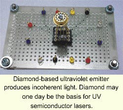
TOKYOResearchers at Tokyo Gas have developed an ultraviolet (UV) emission element based on synthetic diamonds (see photo). Doping the diamonds with boron and turning them into p-type semiconductors causes excitons (electron/hole pairs bound by Coulombic forces) to be formed when current is applied. When these pairs recombine, light at 235 nm is emitted.
To achieve emission, a crystal with extremely high purity and few defects is necessary. Until now, neither natural nor synthetic diamonds could adequately serve this purpose. Conventional diamonds could emit only long-wavelength light caused by impurities and lattice defects.
Tokyo Gas imports a large amount of liquid natural gas. The company has been conducting research on carbon powder extraction from methane, a primary component of natural gas. The successful production of the new UV emission element can be attributed to the high-quality diamonds manufactured using this carbon powder. By subjecting the powder to a high-pressure, high-temperature environment of about 50,000 atmospheres and 1500°C, single-crystal diamonds with a diameter of 2-3 mm were made. Impurities and defects were kept at a minimum by using fine-control mechanisms and melting agents. Plans for making p-n junctions are underway, with the goal of making lasers within the next five years.
Possible applications of such lasers include high-density optical storage and lighting based on UV-stimulated fluorescence. The extreme durability of diamond gives it an advantage over other semiconductor materials with regard to high-output emission, according to the researchers.
Courtesy O plus E magazine, Tokyo
