MICRO-OPTICS: Gigahertz LED reaches high efficiency

The ideal light-emitting diode (LED) for use in fiberoptic communications must be more than just an efficient light source, it also must be capable of modulation at high rates and should be small enough that its output can be efficiently coupled into an optical fiber. An improvement in one of these characteristics often comes at the expense of the others.
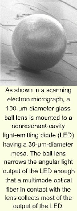
Researchers at IMEC (Leuven, Belgium) have succeeded in producing an LED that excels in all three categories. The device is an oxide-confined gallium arsenide/aluminum gallium arsenide nonresonant-cavity LED in which the thickness of the active layer must be finely tuned to achieve the right balance between efficiency and modulation capability. The addition of a spherical glass microlens tightens the device's angular light output for efficient fiber coupling (see image).
The 870-nm-emitting LED has an outer mesa diameter of 30 µm and an active area—defined by an aperture that confines the electrical current—of 12 to 15 µm. The researchers experimented with active-layer thicknesses of 10, 20, and 30 nm. To increase external quantum efficiency, the surface of the LED was microstructured during fabrication by a method called natural lithography, according to Reiner Windisch, one of the researchers.
"A monolayer of randomly positioned latex spheres is used as a mask for dry etching," he explains. "This produces randomly positioned cylindrical pillars on the surface with wavelength-scale dimensions." After fabrication, the spherical microlens was attached to the device with ultraviolet-curing glue. However, more-manufacturable techniques have already been developed elsewhere to attach ball lenses in large volume, says Reiner.
The IMEC researchers looked at both bit rate and efficiency as a function of the thickness of the active layer. Bit rate was determined by pulsing the devices between a low voltage of 1 V and various higher voltages of 1.5-3.5 V. The maximum achievable bit rate was reached when a measured eye diagram was half as open as at a low bit rate. External quantum efficiency (QE) was measured as the LEDs were being modulated. An active area with a thickness of 10 nm produced 1.2 Gbit/s at an external QE of 20%; a 20-nm thickness produced 1 Gbit/s at 29% external QE; and a 30-nm thickness gave 600 Mbit/s at 32.5% external QE. At an efficiency of less than than 20%, the 10-nm-thick device reached 1.3 Gbit/s. In another device designed for low data rates and with no ball lens, a 120-nm-thick active layer produced an external QE of 40%—the highest ever achieved for an unpackaged LED, according to the researchers.
At a diameter of 100 µm, the glass microlens captures virtually all the light from the LED. While a bare LED emits in a Lambertian pattern, a lensed LED emits such that 50% of the emitted light is confined within a cone having a half angle of 30°. Because this is the acceptance angle of an optical fiber with a numerical aperture of 0.5, the ball lens could be butted up against a multimode fiber so that most of the light is coupled into the fiber.
Although the LED has yet to be coupled to a fiber, calculations show that the addition of the ball lens doubles the coupling efficiency over that of a bare LED, say the researchers. They note that the addition of the ball lens also makes coupling efficiency independent of temperature, in contrast to resonant-cavity LEDs whose angular output changes with temperature.

John Wallace | Senior Technical Editor (1998-2022)
John Wallace was with Laser Focus World for nearly 25 years, retiring in late June 2022. He obtained a bachelor's degree in mechanical engineering and physics at Rutgers University and a master's in optical engineering at the University of Rochester. Before becoming an editor, John worked as an engineer at RCA, Exxon, Eastman Kodak, and GCA Corporation.