Model revises view of quantum-dot function
Supercomputer modeling offers a useful tool for nanoscience when processes within nanosize objects occur at scales below the resolution limits of available imaging technology, and when one wants to look inside the nanostructure where experimental measurement is impossible, according to researchers at the Computational Research Division of Lawrence Berkeley National Laboratory (Berkeley, CA), who used the Seaborg supercomputer at the Berkeley Lab’s National Energy Research Scientific Computing Center (NESRC) to model the dielectric function within a quantum dot, and to substantiate a recently advanced theoretical assertion that the relationship between bandgap energy and dielectric constant on the nanoscale may not be as simple as has been traditionally thought.
Quantum dots change the optoelectronic characteristics of a material by decreasing the size of a particle of that material below the quantum-mechanical wavelength of its electrons, which also boosts the bandgap energy. In bulk gallium arsenide, for instance, the band gap is 1.52 eV, but increases to 2.8 and 3.2 eV in quantum dots consisting of 933 and 465 atoms, respectively, of gallium and arsenic. The mediator of functional change with changing size in a quantum dot is actually the changing exciton energy, which equals the bandgap energy minus the electron hole Coulomb interaction. The latter depends on the dielectric constant, and the average values of dielectric constants over small quantum dots (1 to 5 nm) have been observed to decrease as bandgaps increase, which has led to the broadly accepted assumption that the dielectric constant in a quantum dot is a global parameter determined by the number of atoms in the dot, as is the bandgap energy.
Two years ago, researchers in France questioned this assumption based on theoretical calculations, and suggested that the dielectric constant of a quantum dot is actually the same as that of the bulk material except at the surface of the dot. To test this assertion, Lin-Wang Wang and Xavier Cartoixà at the NERSC created supercomputer models of 933-atom gallium arsenide quantum dots and 465-atom quantum dots in gallium arsenide and silicon and calculated the effect on the microscopic dielectric response caused by a delta potential perturbation introduced in the bulk material and at the dot surface.
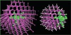
Wang and Cartoixà found that the distribution of charge change around the introduced perturbation was symmetrical within the bulk (left) but was truncated at the surface of the dot (right). Furthermore, when the perturbation was at the interior of the dot, the microscopic charge response was almost the same as in the bulk material. All these indicate that even though the bandgap and the dielectric constant may still be linked in some way, the relationship is not as simple as was previously thought, because the bandgap is a global parameter while the microscopic dielectric response is local. A supercomputer was required to perform the calculations because each one required solving Schrödinger’s equation for a few thousand eigenstates, Wang said. Now that the initial research has been done, however, simpler models can be created to enable easier calculations, and Wang expects that similar methodology will also find use in other areas of nanoscience.
REFERENCE
1. X. Cartoixà and L.-W. Wang, Phys. Rev. Lett. 94(236804) 1 (June 17, 2004).
About the Author
Hassaun A. Jones-Bey
Senior Editor and Freelance Writer
Hassaun A. Jones-Bey was a senior editor and then freelance writer for Laser Focus World.
