With self-assembly as the preferred method of fabrication, quantum-dot lasers are benefiting from high-temperature-grown spacer layers and the use of p-type modulation doping to improve temperature performance.
In comparison to quantum-well lasers, quantum-dot lasers offer the possibility of improved device performance. The electronic states of a quantum dot are fully quantized, resulting in a discrete, atomic-like density of states. For ideal, isolated quantum dots with only one confined electron and one confined hole state, carrier injection occurs only into these states with no thermal excitation possible, resulting in an extremely low and temperature-insensitive threshold current. For real quantum dots-that have multiple confined states and states in the surrounding matrix-the temperature sensitivity will depend on the energetic proximity of these states to the lasing states. An open question is how close the performance of a real quantum-dot laser can approach that of an ideal device.
Self-assembled quantum dots
For laser applications, quantum dots must exhibit a high optical efficiency, be of a sufficiently small size such that the confined states are energetically well-separated, have a high density to provide high gain, exhibit good uniformity, and be fabricated using standard epitaxial techniques. Self-assembled dots satisfy the majority of these requirements.
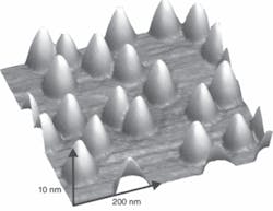
FIGURE 1. Uncapped indium arsenide (InAs) self-assembled quantum dots can be grown on gallium arsenide (GaAs).
Self-assembly occurs when two semiconductors with significantly different lattice constants are grown epitaxially. For example, indium arsenide (InAs) forms small islands, or quantum dots, when grown on gallium arsenide (GaAs; see Fig. 1). The dots are subsequently overgrown with GaAs and a planar surface is quickly reestablished, allowing the growth of further dot layers. Lasers based on self-assembled quantum dots now exhibit threshold current densities a factor of three smaller than comparable quantum-well lasers.
Quantum dot lasers at 1.3 µm
Quantum-dot GaAs-based lasers operating at 1.3-µm provide an attractive alternative to indium phosphide (InP)-based quantum-well lasers, which require the use of more-expensive InP substrates, exhibit poor temperature performance, and for which the fabrication of vertical-cavity surface-emitting lasers (VCSELs) is difficult because of the lack of suitable semiconductor pairs required for the Bragg stacks
Indium arsenide quantum dots grown in GaAs typically emit light at approximately 1.0 µm. To shift the emission to 1.3 µm, either the dot size is increased or the dot environment is modified by growing the dots in an indium gallium arsenide (InGaAs) quantum well. The latter technique results in a higher dot density and is therefore more suitable for laser applications. However, even with this technique, the modal gain of a single dot layer is low, requiring the use of multiple dot layers to achieve sufficient gain. As a consequence, the amount of strained material deposited (both the InAs dots and surrounding InGaAs are strained) is relatively high, and the growth must be carefully optimized to prevent strain relaxation and defect formation.
In a recent report of molecular-beam-epitaxy (MBE) growth of 1.3-µm quantum-dot lasers, it was shown that the growth of the GaAs spacer layer placed between the InGaAs quantum wells is critical for device performance.1 This layer is generally grown at the same temperature as the indium-containing layers, which must be relatively low (approximately 500°C) to prevent indium desorption from the growth surface. Unfortunately, at this temperature the surface mobility of the gallium atoms is low, and hence it is difficult for the GaAs to replanarize the surface. As a consequence, growth of the subsequent layer of quantum dots occurs on a rough surface, with pits acting as preferential nucleation sites. Dots formed at the site of these pits are, on average, larger and can exceed the critical thickness for defect formation. The presence of defective dots appears as a reduced optical efficiency and a higher internal loss and threshold current.
The initial GaAs spacer-layer growth temperature cannot be increased; otherwise, indium is lost from the dots, reducing their emission wavelength. However, by growing the final 35 nm (out of a total of 50 nm) at an elevated temperature of 580°C, the growth surface is effectively planarized by the increased gallium atom mobility, resulting in defect-free dot growth in the subsequent layer. The use of this high-growth-temperature spacer layer (HGTSL) reduces the density of defective dots from about 109 cm-2 to less than 106 cm-2 in a five-layer structure.
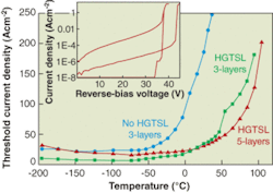
FIGURE 2. Temperature performance of three 1.3-µm quantum-dot laser devices with a 5-mm cavity length improves when the fabrication method includes a high-growth-temperature spacer layer (HGTSL). The reverse-bias characteristics of non-HGTSL and HGTSL quantum-dot laser devices also differs, and can be compared with a quantum-well laser for which the leakage current below 35 V is set by the noise level of the measurement system (inset).
The difference between devices grown with and without HGTSLs is significant (see Fig. 2). Comparing devices with three dot layers, the threshold current density is reduced by a factor of five at room temperature by the inclusion of the HGTSLs. For a non-HGTSL, five-layer device, the defect density is too high to permit room-temperature operation. With HGTSLs, however, operation above 100°C is possible. In similar devices, with three layers of dots and the spacer-layer thickness increased to 70 nm, continuous-wave (CW) room-temperature threshold current densities of 32.5 and 17 A cm-2 are obtained for as-cleaved devices with 5‑mm cavity lengths and for high-reflectivity, coated-facet devices with 2-mm cavity lengths, respectively.2
The incorporation of the HGTSLs also improves the reverse-bias leakage current, indicating that defective dots act as current leakage paths. Because the device with HGTSLs still has a leakage current significantly higher than that observed for a reference 1.0-µm InGaAs quantum-well laser, the HGTSL devices may still contain some defective dots. Improve device performance may result from further growth optimization.
Improving temperature stability
Indium phosphide-based 1.3‑µm quantum-well lasers have a relatively low characteristic temperature (T0) of about 60 K, although this may be increased to about 100 K with the use of indium gallium aluminium arsenide (InGaAlAs) confining layers. In contrast, an ideal quantum-dot laser should have a T0 of infinity. However, in practice, multiple-dot states, states in the surrounding matrix, or nonradiative processes (defect- or Auger-related) act to give a finite T0. Typical T0 values for 1.3‑µm quantum-dot lasers range from 60 K to 140 K.
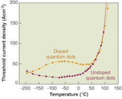
FIGURE 3. The temperature stability of a quantum-dot laser can be improved by p-type modulation doping.
Recently, researchers have achieved an improved T0 by p-type modulation doping of the quantum dots (see Fig. 3).3 When comparing two devices with and without p-type doping over the temperature range of -100°C to +60°C, the doped device displays a reduced temperature sensitivity in comparison to the undoped device. However, above 60°C the temperature sensitivity of the two devices is essentially identical. It is desirable to extend the temperature-insensitive behavior of the doped device to higher temperatures.
Further progress needed?
Optimized 1.3-µm quantum-dot lasers currently exhibit excellent characteristics, with ultralow threshold current densities and high temperature stability at and beyond room temperature. However, further improvements are desirable. The mechanism for the relatively rapid increase of the threshold current at temperatures above 60°C needs to be identified and, if possible, eliminated.
Self-assembled quantum dots exhibit significant size inhomogeneity. As a result, only a subset of the quantum dots contribute to lasing. It is therefore desirable to improve the dot uniformity although it remains unclear whether significant improvements are possible. Modulation rates can be inhibited by the “phonon bottleneck,” in which fast carrier relaxation between the discrete dot states is prevented by the lack of an efficient energy-conserving process. To date, modulation rates of 10 Gbit/s have been reported for 1.3-µm lasers with p-type doping of the quantum dots. In addition, the lifetime of the devices, which contain a considerable amount of highly strained material, needs to be determined.
Finally, there is growing interest in extending operation to 1.55 µm. In fact, 1.5-µm operation for a GaAs-based quantum-dot laser has been achieved by including a relaxed InGaAs layer that modifies the strain environment of the quantum dots.4 The only problem is that the threshold current density is relatively high, approximately 1 kA cm-2, probably a result of defects introduced by the relaxed layer. Other possibilities for increasing the emission wavelength include the addition of small amounts of nitrogen or antimony to the InAs dots to decrease their bandgap.
Gallium arsenide-based quantum-dot lasers operating at 1.3 µm are now available commercially from a number of sources. Over the next few years, continuing performance improvements will dictate whether or not these devices are capable of providing a practical alternative to existing quantum-well lasers.
REFERENCES
1. H. Y. Liu et al., Appl. Phys. Lett. 85, 704 (2004).
2. I. R. Sellers et al., Electron. Lett. 40, 1412 (2004).
3. O. B. Shchekin and D. G. Deppe, Appl. Phys. Lett. 80, 3277 (2002).
4. N. N. Ledentsov et al., Electron. Lett. 39, 1126 (2003).
DAVID MOWBRAY is a reader in the Department of Physics and Astronomy at the University of Sheffield, Sheffield S3 7RH, England; e‑mail: [email protected].


