Optical interconnects aim for faster, smaller, cheaper, and lower power
The challenge for optical interconnects is to span shorter distances at higher speeds, with signals sent through many parallel fibers or waveguides.
Optical interconnection of electronic processors is already standard inside large electronic computers, high-speed switches, and data centers. High-speed signals traveling more than five or six meters are converted into optical data streams at 2.5 or 3.125 Gbit/s, then converted back into electronic form at the receiving end. Connections are made through ribbons of a dozen parallel fibers, each carrying one data stream. The conversion between electronic and optical formats is a bit cumbersome, but it pays dividends. Data rates possible over optical links do not depend strongly on distance, and optics can pack channels more tightly together, avoid electromagnetic interference, and reduce power requirements.
Now developers are trying to push optical interconnects to the higher data rates needed for new generations of computers, while making them practical over even shorter distances. Commercial groups are stepping up the data rate to 10 Gbit/s over a dozen parallel fibers for interconnections spanning several meters or more in switches, routers, high-end servers, and high-end computers. The Defense Advanced Research Projects Agency (DARPA) looks to push even faster speeds and shorter distances. Its chip-to-chip optical interconnects program is targeting channel speeds to 40 Gbit/s and connections between chips or modules installed on the same printed-circuit board. Reaching that target and going further require new types of optical transmitters and receivers that combine low cost, tiny size, and high performance.
A moving target
The concept of optical interconnections inside electronic computers was laid out more than 20 years ago in a paper by Joe Goodman of Stanford University and three colleagues.1 The main reasons it cited for moving from electronic to optical interconnects are still important, says Ravindra Athale, a coauthor of the 1984 paper who now manages DARPA’s chip-to-chip optical interconnects program. Optics don’t dissipate as much heat as high-speed electronic connections. Optics can pack more bandwidth into the same cross section, and don’t suffer the crosstalk due to electromagnetic interference that affects electronic signals. Optical attenuation is virtually independent of frequency, while losses of electronic transmission lines increase with frequency.
Yet the optical interconnect revolution has been slow in coming. Although fiber has compelling advantages over long distances, electronic technology has been a moving target over very short hauls inside cabinets and control centers. Innovative engineering has circumvented the show-stopping electronic bottlenecks that optics researchers had expected would choke electronic transmission speeds as component dimensions shrank and circuit speeds increased. Optics have improved as well, and have succeeded in carving out a niche for interboard transmission of multigigabit data streams through fiber runs of more than five meters. But connections over shorter distances and at lower speeds continue to be made electronically, by copper wires or conductors on chips.
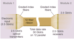
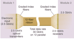
In today’s commercial state-of-the-art optical interconnects output data is aggregated electronically into a dozen streams, each at 2.5 Gbit/s, which are each sent through one fiber in a 12-fiber ribbon cable (see Fig. 1). The short distances needed for optical interconnects allow the use of multimode graded-index fibers, which can transmit signals at 850 nm up to 600 m. Then data is converted into electronic form for distribution within a second module. Standardized modules are available from several vendors.
Suppliers are taking the next logical step, to 10-Gbit/s transmission through 12-fiber ribbons at total data rates to 120 Gbit/s. Agilent Laboratories (Palo Alto, CA) has developed a system based on bottom-emitting 990‑nm vertical-cavity surface-emitting lasers (VCSELs), and bottom-illuminated indium gallium arsenide/indium phosphide (InGaAs/InP) detectors that is flip-chip bonded to integrated circuits and can transmit through 100 m of multimode fiber ribbon.2 The IBM Watson Research Center (Yorktown, NY) has developed a similar system based on top-emitting 850-nm VCSELs and top-illuminated GaAs detectors.3
DARPA pushes state of the art
DARPA wants to take a quantum leap further, continuing an interest in optical interconnection that began with the Strategic Computing Initiative of the mid-1980s. The first projects focused on materials, and looked to develop connections that went through free space rather than fibers. In 1989, DARPA launched the optoelectronic technology consortium, targeting development of systems transmitting 500-Mbit/s signals through 32 parallel fibers, for a total data rate of 16 Gbit/s. Later, DARPA invested heavily in developing VCSELs for transmitters and conducted interconnection-intensive system demonstrations as part of its VLSI (very large scale integration) Photonics program.
Although DARPA’s current program nominally addresses chips, its real target is connecting packaged modules. As computing requirements increase, standard 2-in.-square modules will be sending and receiving data streams of 5 to 10 Tbit/s. “The question is how to do this without burning up the chip or resorting to a technology that is completely nonmanufacturable” because of tight tolerances, Athale says.
The starting point is 1-m transmission of 10 Gbit/s. That’s the bleeding edge for transmission of a single channel using copper technology. Crosstalk between parallel conductors limits copper transmission of multiple channels at that speed, with conductor size and power consumption posing additional problems. DARPA is betting that optics can overcome these problems to pack channels an order of magnitude closer together than electronics. It also hopes to limit power consumption to 50 mW per 10-Gbit/s channel, one-fifth the level of an equivalent electronic link. As DARPA enters the 18-month second phase of the program, its specific target is to transmit 48 parallel 10-Gbit/s channels through a 1-m optical link fabricated on a printed-circuit board.
The biggest challenge is to overcome the costs of converting electronic signals to optical form and back again-these are relatively high for such short links. Athale says transmitters and receivers should be cheap and unobtrusive. That means they must be manufacturable with high yield and good reliability, and compatible with automated assembly processes.
“Receiverless” circuits
Transmitters can be relatively simple; dispersion and attenuation are not serious problems over the short distances involved. The design strategy is to use high transmitter powers to avoid the need for complex receivers. One approach being developed for DARPA by a team led by Larry Coldren of the University of California at Santa Barbara and Joe Campbell of the University of Texas at Austin is based on electroabsorption modulation of a laser that oscillates in the plane of the junction layer. Early demonstrations showed 10-Gbit/s modulation of edge-emitters producing more than 10 mW at 1.54 µm; program goals are data rates to 40 Gbit/s on a single channel, and 980-nm lasers with in-plane oscillation and output coupling through the laser surface. The same team is working on matching "receiverless" circuits in which photodiodes are connected directly to digital logic circuits. Kevin Lear of Colorado State University in Fort Collins is working on direct modulation at up to 40 Gbit/s of VCSELs emitting at 980 nm, where gallium arsenide substrates are transparent, so efficiency is high and laser designs can be simple.
To squeeze transmission lines together more closely than possible in linear arrays, teams at IBM and Agilent are working on a system demonstration called "Terabus" using two-dimensional arrays of VCSELs and detectors containing four rows of devices. The system demonstration is targeting 10 to 15 Gbit/s on all channels. VCSELs and photodiodes have reached 20 Gbit/s, says Dave Dolfi, whose group at Agilent Laboratories (Palo Alto, CA) is developing the optoelectronic components. Demonstration of 40 Gbit/s on one channel is also possible. Devices in each row will be spaced on 250-µm centers, but staggered so across the four rows there is one emitter every 62.5 µm. That spacing is too tight for coupling to a ribbon of fibers, but planar polymer waveguides can be made that narrow. Attenuation is not a big issue because the distance is short, and the waveguides could be fabricated on-or perhaps inside-the printed-circuit board.
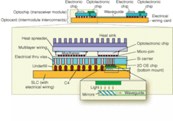
The III-V semiconductor optoelectronics would remain on chips separate from the silicon electronic processors, but packaged within the same 2-in. module. Signals must travel a few millimeters in electronic form, but Athale says that’s not an issue. It’s far simpler than trying to deal with the thermal and packaging problems of integrating optoelectronics onto the same substrate as a standard electronic chip. IBM has developed a packaging system called Optochips, which can be attached with solder bump junctions to a set of multilevel platforms for electronic cards and optical waveguides (see Fig. 2).
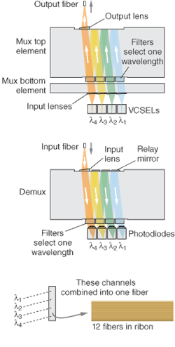
Agilent has also developed a wavelength-division-multiplexed (WDM) system for a nearer-term DARPA project, in which coarse WDM combines four 10-Gbit/s channels onto each fiber in a 12-fiber ribbon.4, 5 The transmitters are an array of 12 columns of VCSELs each consisting of four VCSELs emitting at 990, 1020, 1050, and 1080 nm. Multiplexers combine the four wavelengths for transmission through a single fiber, then a demultiplexer separates them for deliver to a column of photodiodes in a similar 4 × 12 array (see Fig. 3). The detector array is monolithic, but the laser array is made by stacking 12-laser bars fabricated for each of the four wavelengths, which Dolfi says is cheaper and easier to do with today's technology than to fabricate monolithic arrays emitting at all four wavelengths.
Outlook
The applications for parallel optical interconnections have evolved over time. Highly parallel computing with multiple processors proved to be a market too small to bring production costs to a reasonable level. Instead, the telecommunications boom drove down costs of optical interconnects by creating a market for high-performance routers and switches. With the telecommunications market now in the doldrums, the new generation of optical interconnects, with total capacity of 100 Gbit/s and up, may go inside high-performance computers.
On-chip connections will remain electronic, at least for the immediate future. The lack of practical silicon-based light sources remains a problem, even after recent demonstrations of silicon Raman lasers, which require off-chip sources of pump light. Last year a study by Intel’s technology and manufacturing group concluded that optical interconnects might offer some advantages for on-chip signal distribution, but would face steep tradeoffs in cost and performance.6 Intel found that optics offered no significant advantage for on-chip clock distribution. But if DARPA succeeds in driving down the costs of optoelectronic conversion, high-speed, highly parallel optical interconnects will find a market in shorter links, between modules on printed-circuit boards, and between boards within a single equipment shelf.
REFERENCES
1. J. W. Goodman, F. J. Leonberger, S.-Y., Kung, and R. A. Athale, Proc. IEEE 72, 850 (1984).
2. L. A. Buckman Windover et al., J. Lightwave Tech. 22, 2055 (September 2004).
3. D. Kuchta et al., J. Lightwave Tech. 22, 2200 (September 2004).
4. B. E. Lemoff et al., J. Lightwave Tech. 22, 2043 (September 2004).
5. G. Panotopoulos et al., OFC 2005, paper OWH2.
6. Mauro J. Kobrinsky et al., Intel Tech. J. 8, 129 (2004).


