Building on recent demonstrations of assembled photonic-circuit elements made from tin oxide (SnO2) nanoribbons and zinc oxide (ZnO) nanowire waveguides, researchers in the Department of Chemistry at the University of California at Berkeley and the Materials Sciences Division of Lawrence Berkeley National Laboratory (both in Berkeley, CA), and the NASA Ames Research Center (Moffett Field, CA) have demonstrated the delivery of nanosecond light pulses from lasing nanowires through a ribbon waveguide, the routing of different colors through networks of nanoribbons, and conduction of light through abrupt 90° angles in an optical-nanoribbon crossbar grid.1 All these achievements (and the ability of these nanostructures to be used in fluid environments) are prerequisites for using nanowire photonic devices in communications, computing, and sensing applications.
The SnO2 nanoribbons were synthesized via a chemical-vapor transport process: SnO powder was heated in a tube furnace for 90 minutes at 1100°C in flowing argon and the nanoribbons were dry-transferred en masse to oxidized silicon substrates. ZnO nanowires were grown as epitaxial arrays on sapphire substrates by the oxidation of metallic zinc at 800°C using gold as a catalyst and heated in a quartz tube for 30 min in flowing oxygen/argon, while gallium nitride (GaN) nanowires were made by chemical-vapor transport of gallium in a quartz tube containing ammonia/hydrogen and a nickel-coated sapphire substrate heated to 900°C for four hours.
To position the nanoribbons and nanowires under a dark-field microscope, a triple-axis micromanipulator was fitted with a 400-nm-diameter tungsten-tipped probe. Continuous-wave resonant illumination was provided by a helium cadmium (HeCd) laser at 325 nm, and pulsed pumping was provided by the fourth harmonic of Nd:YAG laser at 266 nm with 8-ns pulse duration and 10-Hz repetition rate. Another HeCd laser at 442 nm and laser diodes at 652 and 532 nm supplied visible light for filtering and fluorescence demonstrations.
The researchers first demonstrated the delivery of light pulses through a lasing nanowire into a nanoribbon. In a staggered-bonded configuration where the GaN nanowire (diameter 130 nm, length 65 µm) was held in close proximity to the SnO2 nanoribbon (240 × 260 nm, length 460 µm) by electrostatic forces and interwire adhesion, the nanowire was pumped above its lasing threshold with pulsed UV excitation and produced a Fabry-Perot type spectrum with a full width at half maximum of 0.8 nm at the output of the nanoribbon. For the staggered-bonded configuration, power-transfer efficiencies of approximately 50% were measured with propagation losses through the nanoribbon of about 10 dB/cm.
Spectral separation
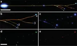
Color separation using nanoribbons is possible because ribbons act as short-pass filters with cutoff wavelengths determined by their cross-sectional dimensions and overall length. To demonstrate, the researchers assembled a network consisting of one long nanoribbon and three shorter ribbons with consecutively thinner dimensions attached as branches. When pumped at 325 nm, the larger-stem nanoribbon emits white light composed of two broad SnO2 photoluminescence bands centered at 495 and 590 nm. The stem emission is transferred selectively to each of the branches and is separated into green, aqua, and blue light components (see figure).
In their final demonstration, a crossbar grid was constructed by overlapping four nanoribbons, with ribbons varying in size from 300 to 400 nm on a side. One ribbon was used as the input, with the other seven ribbon ends used for monitoring. While ribbon-to-ribbon coupling efficiency is less than 5%, photons were detected even after passing through two right-angle junctions and three separate nanoribbon cavities.
Compared to silica waveguides, nanoribbons and nanowires have another significant advantage: their high refractive index (n greater than 2) allows them to guide light within liquids-of extreme importance for on-chip chemical analysis and biological spectroscopy. “We find that nanoribbons function excellently as waveguides in liquid media and provide a unique way to probe molecules in solution or in proximity to the waveguide surface,” says researcher Peidong Yang. “Our results lay the spadework for photonic devices based on assemblies of active and passive nanowire elements and presage the use of nanowire waveguides in microfluidics and biology.”
REFERENCE
1. D. J. Sirbuly et al., Proc. National Academy of Sciences102(22) 7800 (May 31, 2005).
About the Author

Gail Overton
Senior Editor (2004-2020)
Gail has more than 30 years of engineering, marketing, product management, and editorial experience in the photonics and optical communications industry. Before joining the staff at Laser Focus World in 2004, she held many product management and product marketing roles in the fiber-optics industry, most notably at Hughes (El Segundo, CA), GTE Labs (Waltham, MA), Corning (Corning, NY), Photon Kinetics (Beaverton, OR), and Newport Corporation (Irvine, CA). During her marketing career, Gail published articles in WDM Solutions and Sensors magazine and traveled internationally to conduct product and sales training. Gail received her BS degree in physics, with an emphasis in optics, from San Diego State University in San Diego, CA in May 1986.
