10-Gbit/s modulator is fabricated on silicon
Researchers at Luxtera (Carlsbad, CA) have developed a process to fabricate advanced photonic components on silicon using standard CMOS processes. They have fabricated a 10-Gbit/s Mach-Zehnder modulator using the same production line that is used for the PowerPC chips made by IBM (White Plains, NY). Also on the same chip as the modulator are the electronics used to drive the device. This sort of combination and the use of CMOS should greatly simplify and lower the cost of optical transceivers.
Other than the fact that it is fabricated on a silicon-on-insulator wafer, the modulator is conventional in form. To get the optical mode down to a small size, a 0.13-µm lithographic process was used, resulting in ridge waveguides with a 0.1-µm2 cross-sectional area. The device is intended for use at the 1550-nm spectral region, where silicon is optically transparent. The length of the modulator is a relatively short 5 mm-a result of minimizing the voltage-length product. The modulation quality at 10 Gbit/s is high, as evidenced by eye diagrams. Applications include high-throughput memory interconnects, central-processor-unit busses, and cluster interconnects. Contact Gabriele Sartori at [email protected].
Quantum-well IR detector senses at 0.9 and 10 µm
Researchers at the Naval Postgraduate School (Monterey, CA) and Nanyang Technological University (Singapore) have developed a multiple-quantum-well IR photodetector that is sensitive to two widely disparate wavelength bands, one at 0.9 (near-IR) and the other at 10 µm (mid-IR). The sensor may be useful in laser designators (devices that mark a target or spot on a target with a laser spot). Detection of the near- and mid-IR bands occurs through interband and intersubband transitions, respectively.
A structure based on gallium arsenide and indium gallium arsenide was used. An asymmetric quantum well boosted near-IR responsivity at low bias. The amount of indium was adjusted to select a near-IR band of 0.82 to 0.95 µm, while well and step widths, along with indium concentration, were adjusted to achieve a mid-IR band of 9 to 11 µm. With a 0.8-V bias and a 40 K temperature, the responsivities in the near- and mid-IR bands were 0.4 and 1 A/W, respectively; estimated detectivity values were 4.5 × 10⁹ and 1.1 × 1010 cm (Hz)1/2/W, respectively. Contact Gamani Karunasiri at [email protected].
High-resolution retinal implant will combine with natural vision
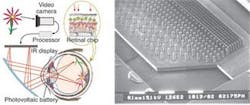
Physicists and eye doctors at Stanford University (Palo Alto, CA) have teamed up to design a retinal implant that may one day bring high-resolution sight to those blinded by retinal degeneration. Degenerative retinal diseases result in death of the eye’s rods and cones; one form of this disease is age-related macular degeneration-the major cause of vision loss in people over age 65. The Stanford retinal prosthesis, which could allow vision to an acuity of 20/80 (sharp enough to allow facial recognition and reading of large fonts), is being tested on rats.
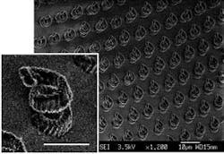
In its first experimental form, the prosthesis is a 3-mm plastic rectangle containing arrays of either pillars or pores (of varying density, for test purposes). Each pillar or pore contains a photovoltaic-powered IR-sensitive photodiode on one side and a cell-stimulating electrode on the other (a separate photovoltaic cell is mounted within the eye to power the prosthesis). The image from an external CCD camera is projected by a goggle-mounted IR light-emitting-diode/liquid-crystal display onto the retina, where the device is activated to stimulate the retina. The goggles transmit visible light so that any remaining natural vision may still be used; the artifical and natural images are overlaid. Early results in rats show no rejection of the implants. Contact Daniel Palanker at [email protected].
Electroluminescent photonic crystal changes color with angle
Three-dimensional photonic crystals (PCs) with photonic bandgaps have spectral-transmission and reflection properties that vary with angle. Although people think of them predominantly in terms of passive optical devices (waveguides, wavelength-selecting filters, and so on), 3-D PCs can be made to be light emitters too; for example, numerous examples of photoluminescent PCs have been created. Now, researchers from the Russian Academy of Sciences (St. Petersburg, Russia) have created electroluminescent PCs driven by an alternating-current electric field. The color of the light emitted from the PC varies from green through yellow to orange as the viewing angle is changed.
Different samples of synthetic-opal PCs were fabricated with silicon dioxide spheres, for example interfilled with gallium nitride (GaN) and zinc oxide (ZnO) doped with manganese (Mn) ions. The example PC was treated in hydrogen sulfide (H2S) at 900°C, producing GaN, ZnS hexagonal, ZnS cubic, and Zn2SiO4 crystal phases. The spheres ranged from 220 to 285 nm in diameter, depending on the sample. Color shifting occurred over an approximately 40° range of angles. Contact Dmitry Kurdyukov at [email protected].
Polymer forms chip-to-chip interconnect
An optical interconnect fabricated from silicone-based polymers has been used to guide 850-nm light between a vertical-cavity surface-emitting laser and a photodiode. A team of researchers from Dow Corning (Midland, MI) and Gemfire (Fremont, CA) fabricated the optical interconnect using standard UV photolithographic techniques.
The photo-defined silicone waveguides measured 100 µm wide by 100 µm high and had a length of 10 cm. After waveguide fabrication, a cladding layer was applied and micromirrors were molded into the cladding before the cladding was cured. The mirrors were formed by bringing a quartz stylus with a 45° tip into contact with the cladding material and then directing UV light into the tip to cure the mirror, as shown. Using this process, groups of 12 waveguides with 250-µm spacing can be faceted in a single pass. The mirrors had very low losses of 0.1 dB per facet, and the complete 10-cm link had an overall insertion loss of 2.5 dB including all the mirrors, waveguides, and reflections. Contact Jon V. DeGroot at [email protected].
Porphyrin nanotubes react to sunlight
Researchers at Sandia National Laboratories (Albuquerque, NM) are hoping to use sunlight to split water molecules and produce hydrogen using porphyrin nanotubes. Very different from the more well-known carbon nanotubes, porphyrin nanotubes are composed of oppositely charged light-absorbing molecules related to chlorophyll that self-assemble in water at room temperature (top figure). Though lacking the high mechanical strength of carbon nanotubes, porphyrin nanotubes have a wider range of optical and electronic properties (including intense resonance-light-scattering ability and photocatalytic activity; bottom figure) that can be exploited to make nanodevices.
When exposed to light, the photocatalytic properties of porphyrin nanotubes can be used to deposit platinum outside the nanotube and grow a nanowire of gold inside the tube, for example. This combination is the beginning of a process that could eventually be used for separation of hydrogen and oxygen from water using visible and UV components of the solar spectrum, although the researchers admit that there are many issues to resolve before this capability can be demonstrated. In addition to this potential application, porphyrin nanotubes may also be applied for use as conductors, semiconductors, chemical sensors, and photonic devices. Contact John Shelnutt at [email protected].
Small pump-wavelength shift causes large output-wavelength shift
Based on a phenomenon called modulational instability (MI), in which an initially continuous-wave pump wave in a single-mode optical fiber breaks up into a periodic wave train, researchers at the University of Auckland (Auckland, New Zealand) and the University of Bath (Bath, England) have produced optical parametric generation tunable over a wide range in a photonic-crystal fiber (PCF). The MI, which produces a pair of sidebands, is caused when the pump is detuned from the zero-dispersion wavelength.
The 1.3-m-long silica PCF has a 1.5-µm-diameter core held by fine silica struts; the zero-dispersion wavelength is about 650 nm. When pumped just below this wavelength, 10-nm tunability in the pump wavelength produces 450 nm of tuning in the sideband. A modelocked, cavity-dumped dye laser with 20-ps pulses at a peak power of 300 W (60 W into the fiber) is used as the pump source. Both pump and output light propagate in the fundamental transverse mode. The low efficiencies of 0.1% to 1 % could be improved by using longer pump pulses and fiber lengths. Contact Rainer Leonhardt at [email protected].
Microlens array enables 3-D multiple-spot micronanofabrication
Using a gradient-index microlens array (MLA) that converts a collimated laser beam into multiple focal points, researchers at The Institute of Physical and Chemical Research (Saitama, Japan), Osaka University (Osaka, Japan), and the Japan Science and Technology Corporation (Osaka, Japan), are fabricating multiple and identical 2-D and 3-D nanostructures through a photopolymerization process.
The MLA is a 10 × 10-mm array of 41 × 41 individual lenses, each with a diameter of 200 µm. The MLA is illuminated by a 100-fs, 600-mW-average-power, 799-nm-wavelength Ti:sapphire pulsed laser operating at 76 MHz. The MLA is moved laterally in two dimensions with a resolution of 100 nm by a stepper motor, while a resin cell is moved up and down by a linear precision actuator with 40-nm resolution. Through two-photon polymerization and by both rotating and laterally moving the MLA as the resin cell is moved down, multiple structures as complicated as 3-D polymer “microsprings” can be fabricated with cord thickness of 1 µm, coil diameter of 5 µm, and height of 8 µm. Contact Hong-Bo Sun at [email protected].
Piezoelectrically actuated tunable VCSEL is modeled
Various microelectromechanical-system (MEMS) tunable vertical-cavity surface-emitting lasers (VCSELs) have been developed that use either electrostatic or thermal actuation mechanisms. Capacitive actuation requires large tuning voltages and results in limited tuning ranges. Thermal actuation suffers from low actuation speed and presents difficulties in fabrication. Using piezoelectric actuation to eliminate electrostatic problems and increase tuning range, researchers from the Department of Electrical Engineering at the University of California, Berkeley (Berkeley, CA) have developed a theoretical model of a 980-nm VCSEL with a 35‑nm tuning range that requires only a 3-V direct-current power supply.
The tunable VCSEL is a monolithic structure that relies on a piezoelectrically actuated cantilever beam, comprised of alternating aluminum gallium arsenide layers (specifically, Al0.1Ga0.9As and Al0.8Ga0.2As). The actuation varies the size of an air gap between the active region of the structure and the top distributed Bragg reflector beam layers to shift the Fabry-Perot mode and the lasing wavelength of the VCSEL. The actuation has a linear response and permits bidirectional actuation with larger tuning ranges at low voltage levels-important features for realizing use of MEMS-tuned VCSELs for optical communication systems and chip-scale atomic clocks.
Contact Gianluca Piazza at [email protected].


