Standing-wave spectroscopy probes buried nano-interfaces
Giant magnetoresistance (GMR), a 20% to 50% change in electrical conductivity caused by the electron interactions across interfaces between magnetic and nonmagnetic metals in the presence of a magnetic field, is routinely used in computer-disk read heads for high-density data storage. It is also just one of many highly useful nanoscale interface processes that are not thoroughly understood.
Scanning transmission electron microscopy (STEM) effectively probes buried nanoscale interfaces after they have been sectioned and thinned, but researchers at the University of California-Davis (UC Davis), Lawrence Berkeley National Laboratory (LBNL; Berkeley, CA), and the IBM Almaden Research Center (San Jose, CA) are developing a nondestructive spectroscopic probe based on soft x-ray excitation of photoemissions.1, 2
Nondestructive visualization of materials and processes at interfaces between layers that are only a few atoms thick is important because layered nanostructures are expected to play a critical role in enabling the next generation of magnetic read heads for high-density data storage, as well as the development of magnetic random-access memory (MRAM) chips to store data using electron spin rather than charge. Such “spintronic” MRAM chips offer the possibility of “instant-on” computers with far less power consumption, much larger storage, and much faster information access than is currently available.
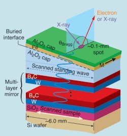
By reflecting a circularly polarized soft x-ray beam generated at the LBNL Advanced Light Source off a nanoscale multilayer mirror, the research team led by Charles Fadley, a physics professor at UC Davis who is also affiliated with the LBNL Material Sciences Division, has devised a unique way to probe buried interfaces via standing waves. The standing wave, generated by Bragg reflection from the mirror oscillates normal to the mirror, enables spectroscopic interrogation of nanomaterials grown on top of the mirror surface.
“With soft x-ray standing waves we can, for the first time, look at multilayered nanostructures using a tour de force of all the relevant spectroscopy techniques, including photoelectron, x-ray emission, and x-ray absorption techniques,” Fadley said. “So we can nondestructively analyze buried interfaces for atomic composition and for chemical, magnetic, and electronic structures.”
Fadley’s research team, which also included See-Hun Yang, currently at the IBM Almaden Research Center (San Jose, CA), and Bongjin Simon Mun at LBNL, as well as Stuart Parkin at Almaden, first used the method to study the GMR effect at an iron-chromium bilayer by depositing a wedge-shaped sample atop the mirror such that horizontal scanning of the 4-nm-period standing wave effectively scans the probe vertically through the interface. Data thus obtained enabled derivation of layer thickness and interface mixing-roughness scales, as well as derivations of positions and widths of regions with increased or decreased ferromagnetic alignment.
Even though the magnetically altered regions in both metals were only one or two atomic layers thick, the researchers observed that the normally antiferromagnetic chromium became ferromagnetic just below the center of the interface but with antiparallel magnetic alignment to the iron, based on photoemissions from 2p and 3p atomic levels. They also noted, based on spectra from 3s atomic levels, that local spin moments on iron and chromium atoms do not change on crossing the interface.
Additional application areas being pursued by the group include probing multilayer structures in magnetic and semiconductor materials, studying self-assembled monolayers, and ultimately performing 3-D spectromicroscopy.
REFERENCES
1. S.-H. Yang et al., Synchrotron Radiation News 17(3) 24 (May/June 2004).
2. S.-H. Yang et al., J. Physics: Condensed Matter 14, L407 (2002).

