Orbital Angular Momentum: Laser-direct-written waveguides enable on-chip twisted light propagation
The orbital angular momentum (OAM) carried by twisted light provides an added degree of freedom that can be exploited to expand the bandwidth of modern fiber-optic communications systems. Recognizing that bulk optical and fiber-optic systems are increasingly being integrated into chip-based photonic systems, researchers at Shanghai Jiao Tong University (Shanghai, China) have been able to develop laser-direct-written on-chip waveguides that transmit OAM beams while maintaining signal integrity. The team also demonstrated both on-chip and off-chip coupling—attributes necessary to producing chip-based OAM systems for high-bandwidth integrated classical and quantum communication networks.
Donut waveguides
Knowing that the typical transverse intensity pattern of an OAM beam is donut-shaped, the researchers created a waveguide with a donut-shaped cross-section that is cylindrically symmetric. And, understanding that total internal reflection can lead to polarization anomalies such as phase shifts at index discontinuities, the researchers were able to design a waveguide through solution of Maxwell’s equations for OAM modes using a first-order perturbative analysis to create a three-dimensional, femtosecond-laser-direct-written waveguide designed to preserve OAM mode integrity.
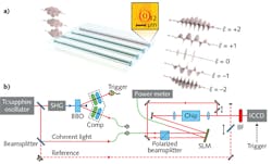
For a 19.64 mm donut-shaped waveguide within a chip, OAM light is coupled in through polished ends of the chip and then measured after interfering with a Gaussian beam. The resultant spiral interference patterns are obtained directly by a CCD camera. The chirality and the number of arms in the measured interference patterns can clearly tell the topological charge of the OAM light. To be specific, the clockwise (counterclockwise) chirality indicates the positive (negative) topological charge, and the number of arms indicates the order.
The waveguide designed for the experiments supports OAM0, OAM+1, and OAM-1 modes. Analysis of higher-order modes was made possible by optimizing the donut-shaped structure in terms of its size and refractive index distribution.
The concept of coupling OAM modes into and out of a photonic chip is shown schematically (a); the donut waveguide maintains the integrity of various OAM modes as measured by the experimental setup (b). (Image credit: Shanghai Jiao Tong University)
For experiments with both standard low-order modes and higher-order modes (see figure), it was found that the waveguide transmitted lower-order modes with an approximate 60% efficiency, meaning that OAM light can be easily mapped into and out of the chip (the total loss—including the transmission process—is only 40%). However, this efficiency drops rather dramatically to around 25% for higher-order modes because of the fact that the OAM waveguide hasn’t yet been optimized to support higher-order modes.
“Our work provides the first photonic chip being capable of supporting OAM modes, which opens up an entirely new field, ‘twisted-light-inside integrated photonics,’ not only for optical communications, but also for optical processing, imaging, and quantum computing,” says Xianmin Jin at Shanghai Jiao Tong University. “To simultaneously support many more OAM modes is very likely; in fact, we are working on extending the supported modes to very high order and have recently obtained results that are very encouraging. Another fascinating thing is to directly generate OAM light inside our OAM waveguide chip; however, this mission is much more challenging.”
REFERENCE
1. Y. Chen et al., Phys. Rev. Lett., 121, 233602 (Dec. 7, 2018).

Gail Overton | Senior Editor (2004-2020)
Gail has more than 30 years of engineering, marketing, product management, and editorial experience in the photonics and optical communications industry. Before joining the staff at Laser Focus World in 2004, she held many product management and product marketing roles in the fiber-optics industry, most notably at Hughes (El Segundo, CA), GTE Labs (Waltham, MA), Corning (Corning, NY), Photon Kinetics (Beaverton, OR), and Newport Corporation (Irvine, CA). During her marketing career, Gail published articles in WDM Solutions and Sensors magazine and traveled internationally to conduct product and sales training. Gail received her BS degree in physics, with an emphasis in optics, from San Diego State University in San Diego, CA in May 1986.
