3D-printed nanophotonic lens improves directivity of nanowire’s light emission
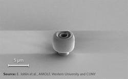
Scientists at the research institute AMOLF (Amsterdam, Netherlands) have developed and fabricated a 3D nanophotonic lens in collaboration with Western University (London, ON, Canada) and the City University of New York. Using a Photonic Professional microfabrication system from Nanoscribe (Eggenstein, Germany), the researchers printed an extremely small lens over a 6-µm-long, 80-nm-diameter gallium arsenide nanowire that acts as a broadband (750–900 nm) light emitter. The combination of nanolens and nanowire enables focused light emission, in contrast to the divergent (0.9 numerical aperture) emission of the nanowire itself.
Highly direction-sensitive nanoscale emitters and sensors offer potential in many fields of application. This is the case for optical quantum computers, as well as for solar cells with nanoscale structured areas or surfaces. However, the enhancement of directivity on nanoscale devices is a major technical challenge. In this work, researchers applied an evolutionary algorithm to design a complex 3D geometry with subwavelength features down to nearly 200 nm. The 3D design uses nanoscale interference effects to achieve a high directivity. The lens, which is about 6 µm in diameter, has a calculated directivity of 101 for a point source, and 67 for the finite-source nanowire emitter. Directivity is defined as the light emission at one angle relative to the mean light emission over all angles. Measured output half-angle was 3.5°, or a numerical aperture of about 0.06, with a directivity of 22—this number could be boosted more towards its theoretical value with better alignment of the lens to the nanowire, say the scientists. Reference: E. Johlin et al., Nat. Commun. (2018); doi:10.1038/s41467-018-07104-1.

John Wallace | Senior Technical Editor (1998-2022)
John Wallace was with Laser Focus World for nearly 25 years, retiring in late June 2022. He obtained a bachelor's degree in mechanical engineering and physics at Rutgers University and a master's in optical engineering at the University of Rochester. Before becoming an editor, John worked as an engineer at RCA, Exxon, Eastman Kodak, and GCA Corporation.
