Silicon LED is efficient at room temperature
Current light-emitting diodes (LEDs) are based on gallium arsenide and are incompatible with silicon-based circuits, which has created a bottleneck for further circuit-miniaturization efforts. According to one estimate, five years from now this interconnectivity problem could stall efforts to boost computer chip processing power and speed.
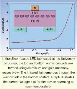
While the ideal solution would be to build the optical emitter from silicon to ensure its compatibility with standard silicon-based ultra-large-scale integration (ULSI) technology, the indirect energy bandgap of bulk silicon makes it extremely inefficient as a light source. In essence, the fast nonradiative recombination routes in the material dominate the slower radiative routes. At room temperature, radiative emission is basically nonexistent. This said, there are reports out of the University of Surrey (Surrey, England) that engineering researchers have found a way around the bandgap problem. The result is a prototype silicon-based LED almost as efficient at room temperature as conventional LEDs made from other semiconducting materials (see figure).
To compare their nonoptimized silicon-based device to conventional optimized LEDs, the scientists measured the external quantum efficiency of the unpackaged planar device based on light emitted through the back window. With a 100-mA forward current, the silicon-based LED emitted 19.8 µW of light according to Kevin Homewood, a project team member from the university's school of electronic engineering, information technology, and mathematics. This translates to an external quantum efficiency of (2.0 ± 0.1) x 10-4 at room temperature. Add in the 80 µW of edge emission from the device, and efficiency jumps to 10-3.
For comparison, Homewood reports that a conventional gallium-arsenide infrared (IR) LED will have external efficiencies approaching 10-2. He notes, though, that commercial packaging of these devices can improve upon that by a factor of 15 or so. The quantum efficiency of the prototype silicon-based LED is thus already within about a factor of three of the efficiencies possible with conventional optimized LEDs. Future research could improve the efficiency.
The Surrey scientists stress that they built the LED using standard silicon processing techniques. The fabrication process differs from prior research efforts in that boron was implanted into the silicon to act as both a dopant to form a p-n junction and a means of introducing dislocation loops. These defects introduce a local strain field in three dimensions that modifies the band structure and provides spatial confinement of the charge carriers. As a result, the silicon outside the loops is free to bring charge carriers to the confining regions, allowing room-temperature electroluminescence at the band gap. Compatibility with standard ULSI technology is ensured because boron-ion implantation is a common step in the fabrication process for silicon devices.
According to Homewood, the fabrication technique developed at Surrey is not limited to silicon. The use of silicon carbide instead of silicon, for example, could allow the fabrication of devices that span the near-IR—including the 1.3- and 1.5-µm regions important for telecommunications—and also up to the ultraviolet region.
REFERENCE
- Wai Lek Ng et al., Nature, 410, 192 (March 8, 2001).
Paula Noaker Powell | Senior Editor, Laser Focus World
Paula Noaker Powell was a senior editor for Laser Focus World.
