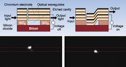
These days, concepts for microelectromechanical systems (MEMS) optical switches intended for fiberoptic networks are legion. Desirable qualities for these devices include low power consumption, high switching speed, high reliability, compactness, and ease of fabrication. The concept is key: some qualities are very hard to achieve for certain designs. Researchers at the Center for Research and Education in Optics and Lasers (CREOL; Orlando, FL) aimed to satisfy as many needs as possible with a design based on a cantilevered waveguide-carrying beam (top left). The 1 x 2 switch is straightforward to fabricate and has been cycled more than 300 million times with no degradation.
The beam—which is 500 µm long, 400 µm wide, and 6 µm thick—contains two waveguides displaced vertically from each other by 4 µm. A voltage applied between the beam and the substrate causes the beam to electrostatically deflect downward, contacting the substrate along part of the beam's length, shifting one output waveguide away from an input waveguide and moving the second output waveguide in front of it (top right). As a result, light is switched from one output waveguide to the other (bottom). The single-mode waveguides are made from silicon oxynitride films and are separated by, among other layers, a 100-nm-thick chromium film that serves as one of the electrostatic electrodes.
To make the device, the beam structure is deposited on a 4-µm-thick layer of silicon dioxide, itself grown on a silicon wafer. The beam's lateral shape is defined by reactive ion etching through openings in a photolithographically patterned chromium layer. The silicon dioxide is then removed from under the beam by isotropic wet etching. The resulting open layer under the beam defines its precise 4-µm movement range. The accuracy of the layers in the beam produces a waveguide spacing accurate to 1%, says Patrick LiKam Wa, one of the researchers. The optical design itself is more tolerant, able to function properly even with a 5% inaccuracy in waveguide spacing, Wa adds.
The electrostatic attraction voltage averaged 25 V, while the release voltage averaged 15 V. Based on measurements of the dynamic response of the switch when driven by a 1-kHz square wave, the switching time response in attraction mode was approximately 90 µs. Crosstalk between channels was measured to be -24 dB. Further advantages of the switch include independence of input wavelength and polarization, and transparency to the bit rate and modulation format.
About the Author
John Wallace
Senior Technical Editor (1998-2022)
John Wallace was with Laser Focus World for nearly 25 years, retiring in late June 2022. He obtained a bachelor's degree in mechanical engineering and physics at Rutgers University and a master's in optical engineering at the University of Rochester. Before becoming an editor, John worked as an engineer at RCA, Exxon, Eastman Kodak, and GCA Corporation.
