SUBWAVELENGTH-SIZED LASERS: Electrically pumped nanolaser works at room temperature
A research team at Arizona State University (ASU) led by Cun-Zheng Ning has created an electrically pumped continuous-wave nanolaser that reliably operates at room temperature.1 Previously, electrically powered nanoscale lasers have been able to operate effectively only in cold temperatures or have emitted only pulsed light. Researchers in the field have been striving to get them to perform reliably at room temperature, a step that would pave the way for their use in a variety of practical applications.
Ning has been among engineers and scientists across the world attempting to fabricate a workable nanolaser with a volume smaller than its wavelength cubed (λ3)—an intermediate step toward further miniaturization of lasers. The new metal-cavity laser emits at a wavelength of 1591 nm and has a cavity volume of only 0.67 λ3. Its room-temperature linewidth of 0.5 nm corresponds to a cavity Q value of 3182.
Ning’s team started looking for solutions almost seven years ago, before he joined ASU, with his then-postdoctoral assistant, Alex Maslov, who is currently a scientist with Canon USA. While working at NASA’s Ames Research Center (Moffett Field, CA), they proposed a semiconductor wire coated with a silver shell. They showed that such a core-shell structure enabled smaller nanolasers.
About four years ago, working with Martin Hill, a former professor at Eindhoven University of Technology in the Netherlands, the team developed the thinnest nanolaser capable of operating at low temperatures. Two years ago, with the aid of Ning’s student, Kang Ding, they were able to raise the operating temperature to 260 K.
More recently, the team demonstrated a device that could operate at room temperature, but the overheating led to imperfect device operation. These most recent results, however, demonstrate an eightfold improvement over previous results from a year ago, finally providing an unambiguous demonstration of continuous electrically driven operation of a laser at room temperature, Ning says.
Near-single-crystal silver
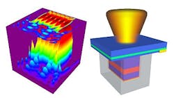
The laser’s structure is made of a rectangular indium phosphide/indium gallium arsenide/indium phosphide (InP/InGaAs/InP) core and a silicon nitride (SiN) insulating layer, all enclosed in a silver cavity shell. Because metal cavities have inherently high losses, the researchers spent time optimizing the structure’s geometry (in particular, the SiN thickness) and the fabrication process, minimizing any imperfection.
One way to lower optical loss is to improve the quality of the silver deposition and post-annealing processes. Doing this, the group was eventually able to achieve near-single-crystal silver quality, producing silver with grain sizes up to 1 μm, which is about the size of the whole laser.
At a temperature of 294 K, the laser showed a threshold around 1.1 mA and an intensity increasing linearly with injection current above the threshold. Below threshold the full width at half maximum (FWHM) linewidth was 6.8 nm, corresponding to a Q factor of 235; above threshold at 2.02 mA, the linewidth dropped to 0.5 nm. The far-field emission was mostly linearly polarized along the longer direction of the cavity’s rectangular output area.
“In terms of fundamental science, it shows for the first time that metal heating loss is not an insurmountable barrier for room-temperature operation of a metallic cavity nanolaser under electrical injection. For a long time, many doubted if such operation is even possible at all,” says Ning.
Remaining challenges
One potential use for such nanolasers is as a building block in active metamaterials, which compensate (or more than compensate) for optical loss by emitting light in phase with that traveling in the metamaterial. Ning says many challenges remain in efforts to integrate nanolasers into a photonic on-chip platform, as well as to prolong the lifetime of laser operation and to further develop the capabilities of such devices. In addition, the physical mechanisms involved in the interaction of photons with metallic structures on small scale are not yet fully understood.
REFERENCE
1. K. Ding et al., Opt. Exp., 21, 4, 4728 (2013).

John Wallace | Senior Technical Editor (1998-2022)
John Wallace was with Laser Focus World for nearly 25 years, retiring in late June 2022. He obtained a bachelor's degree in mechanical engineering and physics at Rutgers University and a master's in optical engineering at the University of Rochester. Before becoming an editor, John worked as an engineer at RCA, Exxon, Eastman Kodak, and GCA Corporation.
