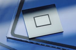
Laser-based glass soldering packages temperature-sensitive glass/glass and glass/ceramics
Aachen, Germany--To package temperature-sensitive glass/glass and glass/ceramics components, especially those with large substrate surfaces to be sealed, a laser-based joining process that uses glass solder is becoming more and more significant. The Fraunhofer Institute for Laser Technology (ILT) is developing the appropriate irradiation strategies and processing heads to achieve this.
The advantage of the laser-based joining process is that the laser beam is able to apply energy to a limited space in order to melt the glass solder precisely, thus generating a bond with long-term, stable hermeticity.
Related: Laser glass soldering provides low-temperature hermetic seal
Sensitive component groups such as optical sensors in medical technology, OLED components or dye solar cells require reliable encapsulation so that neither water nor oxygen can reach the interior of the component. Conventionally, such components are joined with anodic or glass-frit bonding or are simply glued together. These bonds, however, are not stable enough over the long term. In addition, the entire component group is heated when it is bonded, which is why the process is not suitable for bonding temperature-sensitive components.
Energy goes entirely to glass solder
In laser-based glass soldering, the laser beam is guided over the workpiece and applies the energy solely into the glass solder itself to melt it. The substrates to be joined are heated only via heat conduction to wet them; this way, the overall heating of the component group can be reduced to a minimum.
One radiation approach for this is quasi-simultaneous laser soldering: a very fast 2D scanner system guides the laser beam over the solder contour many times at a high speed and evenly heats the entire glass solder contour up to processing temperature by means of a laser power-time profile. After both joining pairs have been bonded, the temperature in the processing zone is lowered according to the profile without creating stress.
Quasi-simultaneous laser soldering is technically restricted by the maximum processing field size of the focusing optics, and is also limited, from an economic point of view, by the laser power required—for example, 1 kW or more is required when substrate sizes of 100 x 100 mm² are joined. Current processing approaches unify the resource-efficient energy input of this quasi-simultaneous process guidance with the size and geometry freedom of continuous processing optics.
New approach
So-called "contour soldering with energy input adapted laterally to feed movement" enables, for the first time, large substrates to be joined at significantly lower laser power. For contour soldering, continuous-beam sources run at a power of less than 100 W, independent of the substrate sizes to be joined.
The team at the Fraunhofer ILT will design the entire production chain for its partners. This ranges from the initial steps to prepare the process (such as the selection of an appropriate glass solder), through the application of the glass solder by means of screen printing, all the way to the pre-vitrification of the pairs to be joined in a convection oven. Especially for laser-based glass soldering, the researchers have developed processing heads as well as positioning and clamping technologies to guarantee homogenous and reproducible packaging in either ambient or inert protective gas atmospheres.
Fraunhofer ILT at the Hannover Messe
In Hall 17 at the IVAM joint stand C50.13 at the Hannover Messe from April 8 to 12, 2013, ILT experts will be exhibiting component groups that were joined using laser-based glass soldering: for example, sensor housings with bonds of glass/silicon and glass/ceramics as well as glass/glass bonds with ITO layers.
About the Author
John Wallace
Senior Technical Editor (1998-2022)
John Wallace was with Laser Focus World for nearly 25 years, retiring in late June 2022. He obtained a bachelor's degree in mechanical engineering and physics at Rutgers University and a master's in optical engineering at the University of Rochester. Before becoming an editor, John worked as an engineer at RCA, Exxon, Eastman Kodak, and GCA Corporation.

