Molybdenum disulfide speeds up amorphous Si detector for medical imaging
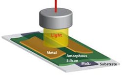
Berkeley, CA--Two engineers at the University of California, Berkeley (UC Berkeley) have created an amorphous silicon (a-Si) metal-semiconductor-metal heterojunction photodetector with added molybdenum disulfide (MoS2) that they say could speed up medical imaging at low cost.1 Molybdenum disulfide is well-known as a lubricant sold in auto-parts shops.
Many photodetectors in large-area imaging devices use a-Si because it absorbs light well and is relatively inexpensive to process. But a-Si has defects that prevent the fast, ordered movement of electrons, leading to slower operating speeds and more exposure to radiation. Getting better performance requires more expensive, high-temperature processing, adding to the price tag of the imaging device.
Sayeef Salahuddin and Mohammad Esmaeili-Rad solved this problem by pairing a thin film of MoS2 with a sheet of a-Si. By forming a diode with the a-Si, the MoS2 allows the photogenerated electrons it collects to travel ten times faster through the a-Si. The detector has a photoresponsivity of 210 mA/W for green light -- two to four times higher than usual for a-Si devices.
The researchers say that because these materials are easy and inexpensive to handle, the cost of speeding up photodetectors would be minimal. Unlike conventional semiconductors like Si, MoS2 consists of individual nanosheets that can be torn off like pages in a book. These sheets can be used to make thin, novel electronic devices or to improve existing ones.
The National Science Foundation and the Defense Advanced Research Projects Agency helped support this work. Esmaeli-Rad's postdoctoral fellowship is supported by the Natural Sciences and Engineering Research Council of Canada.
REFERENCE:
1. Mohammad R. Esmaeili-Rad and Sayeef Salahuddin, Scientific Reports 3, article number 2345, 2 Aug. 2013: doi:10.1038/srep02345.

John Wallace | Senior Technical Editor (1998-2022)
John Wallace was with Laser Focus World for nearly 25 years, retiring in late June 2022. He obtained a bachelor's degree in mechanical engineering and physics at Rutgers University and a master's in optical engineering at the University of Rochester. Before becoming an editor, John worked as an engineer at RCA, Exxon, Eastman Kodak, and GCA Corporation.
