NIST researchers achieve chip-scale bidirectional optical frequency conversion between 980 and 1550 nm
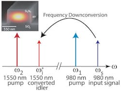
| In frequency downconversion, a 980 nm input signal is frequency-shifted to the 1550 nm wavelength band through the application of two strong pump lasers. The reverse process of upconversion was also demonstrated. Inset: A scanning electron micrograph (SEM) of the cross-section of a silicon nitride waveguide designed for the frequency conversion is shown with a simulation of the device's optical field profile superimposed. (Image: NIST) |
Gaithersburg, MD, College Park, MD, and Pasadena, CA--Researchers from the National Institute of Standards and Technology (NIST), the University of Maryland, and the California Institute of Technology (Caltech) have created a chip-scale optical frequency converter that uses four-wave-mixing Bragg scattering in silicon nitride waveguides on silicon substrates to upconvert and downconvert between the 980 nm and 1550 nm wavelength regions.1 The device can be used to link system components that perform optimally at their specific tasks, but operate at different wavelengths; components can include quantum dots (QDs) and even naturally occurring atoms such as neutral alkali atoms.
Earlier work had demonstrated conversion over a range of a few nanometers with conversion efficiencies reaching a few percent; here, the authors extended the conversion range to nearly 600 nm. This improvement was made possible by the nature of the four-wave-mixing process, in which the locations of the two pump fields, input signal, and converted signal can be rearranged while preserving the requirements of energy and momentum conservation.
The authors demonstrated that the process was bidirectional (signals can be converted from 980 nm to 1550 nm and back), and developed designs to interface light at wavelengths all the way down to 637 nm -- characteristic of the nitrogen vacancy center in diamond -- with the 1550 nm band. (Diamond vacancies are one of the most important potential components in room-temperature quantum optical systems.) The technique requires low pump powers of less than 50 mW.
Future work will be focused on significantly increasing the conversion efficiency levels of these devices by optimizing the geometries and using resonant cavities.
Source: http://www.nist.gov/cnst/nanophotonics_freq_conv_interface.cfm
REFERENCE:
1. I. Agha et al., Optics Express 21, p. 21628 (2013).
