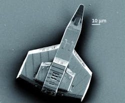
Micro-nanostructure 3D printer from Nanoscribe uses new, fast laser lithography method
Eggenstein-Leopoldshafen, Germany--Nanoscribe GmbH (www.nanoscribe.de), a spinoff of Karlsruhe Institute of Technology (KIT), has developed what it calls the world's fastest three-dimensional (3D) micro- and nanostructure printer. The printer is based on a novel laser lithography method and can be used, among numerous other applications, to print polymer waveguides reaching data transfer rates of more than 5 terabits per second.
By means of the new laser lithography method, printing speed is increased by factor of about 100. This increase in speed results from the use of a galvo mirror system, a technology that is also applied in laser show devices or scanning units of CD and DVD drives. Reflecting a laser beam off the rotating galvo mirrors facilitates rapid and precise laser focus positioning. “We are revolutionizing 3D printing on the micrometer scale. Precision and speed are achieved by the industrially established galvo technology. Our product benefits from more than one decade of experience in photonics, the key technology of the 21st century,” says Martin Hermatschweiler, the managing director of Nanoscribe GmbH.
The direct laser writing technique underlying the 3D printing method is based on two-photon polymerization. Just as paper ignites when exposed to sunlight focused through a magnifying glass, ultrashort laser pulses polymerize photosensitive materials in the laser focus. Depending on the photosensitive material chosen, the exposed or unexposed volume only is dissolved. After a developer bath, these written areas remain as self-supporting micro- and nanostructures.
By means of the galvo technology, 3D micro- and nanostructures can be printed rapidly and, hence, on large areas in principle. At highest resolution, however, the scanning field is limited physically to a few hundreds of microns due to the optical properties of the focusing objective. Just as floor tiles must be joined precisely, the respective scanning fields have to be connected seamlessly and accurately. By the so-called stitching, areas can be extended nearly arbitrarily.
"The success of Nanoscribe is an example of KIT's excellent entrepreneurial culture and confirms our strategy of specifically supporting spin-offs. In this way, research results are transferred rapidly and sustainably to the market," says Peter Fritz, KIT VP for Research and Innovation. In early 2008, Nanoscribe was founded as the first spinoff of KIT and has since established itself as a technology leader in the area of 3D laser lithography. Last year, 18 spinoffs were established at KIT. Work in the area of photonics concentrates on replacing conventional electronics by optical circuits of higher performance.
Karlsruhe Institute of Technology (KIT) is a public corporation according to the legislation of the state of Baden-Württemberg. It fulfills the mission of a university and the mission of a national research center of the Helmholtz Association. KIT focuses on a knowledge triangle that links the tasks of research, teaching, and innovation.
SOURCE: Karlsruhe Institute of Technology; http://www.kit.edu/visit/pi_2013_12589.php

Gail Overton | Senior Editor (2004-2020)
Gail has more than 30 years of engineering, marketing, product management, and editorial experience in the photonics and optical communications industry. Before joining the staff at Laser Focus World in 2004, she held many product management and product marketing roles in the fiber-optics industry, most notably at Hughes (El Segundo, CA), GTE Labs (Waltham, MA), Corning (Corning, NY), Photon Kinetics (Beaverton, OR), and Newport Corporation (Irvine, CA). During her marketing career, Gail published articles in WDM Solutions and Sensors magazine and traveled internationally to conduct product and sales training. Gail received her BS degree in physics, with an emphasis in optics, from San Diego State University in San Diego, CA in May 1986.
