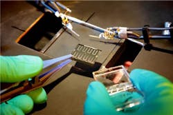
Improved fabrication method for kesterite thin-film solar cells may widen their use
Luxembourg City, Luxembourg--Thin-film solar cells made from copper-zinc-tin-chalcogenide kesterites are not only efficient (up to about 10%), but low in cost too. This is because all the raw materials needed to fabricate them are cheap and abundant.
One barrier to the wider use of these kesterites for thin-film photovoltaics is unwanted loss of tin from the thin film during fabrication at elevated temperatures, which ruins the ability to precisely control the film composition and homogeneity.
Simpler precursor film
Researchers at the Université du Luxembourg have overcome this problem by learning more about the reactions occurring during formation of the thin-film material.1 As an added benefit, they have figured out how to begin the manufacturing process with a precursor film of only copper and zinc, rather than a film containing all four materials. This allows the addition of the other materials during fabrication to be simplified, as material proportions become much easier to monitor.
"With this first success, we are now able to understand the further limitations of these solar cells," says Susanne Siebentritt, head of the Laboratory for Photovoltaics. "This will help us to improve the efficiency further."
The Laboratory for Photovoltaics of the University of Luxembourg is a group of researchers developing new materials and processes for solar cells. The laboratory focuses also on furthering the physical understanding of the materials and interfaces involved in these solar cells.
REFERENCE:
1. Alex Redinger et al., J. Am. Chem. Soc., 133 (10), p. 3320 (2011); Publication Date (Web): February 18, 2011.
Subscribe now to Laser Focus World magazine; it’s free!

John Wallace | Senior Technical Editor (1998-2022)
John Wallace was with Laser Focus World for nearly 25 years, retiring in late June 2022. He obtained a bachelor's degree in mechanical engineering and physics at Rutgers University and a master's in optical engineering at the University of Rochester. Before becoming an editor, John worked as an engineer at RCA, Exxon, Eastman Kodak, and GCA Corporation.
