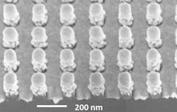
Plasmonic-nanodot SERS sensor detects individual molecules
Princeton, NJ--Engineers at Princeton University have invented an extremely sensitive surface-enhanced Raman scattering (SERS) sensor that can detect samples as small as a single molecule.1 Rather than relying just on a conventional SERS scattering metal surface or on metal nanoparticles, the sensor contains a chip studded with uniform rows of nanopillars made of metals and insulators.
In Raman scattering, a beam of monochromatic light is focused on a target; the reflected light from the object contains two extra wavelengths ("Raman-shifted" light). The shifted wavelengths are unique to the molecular make-up of the substance, providing a potentially powerful method to determine the identity of the substance. A patterned metal (usually gold or silver) surface on the target enhances the Raman-shifted signals.
"Raman scattering has enormous potential in biological and chemical sensing, and could have many applications in industry, medicine, the military, and other fields," said Stephen Chou, who led the Princeton research team. "But current Raman sensors are so weak that their use has been very limited outside of research. We've developed a way to significantly enhance the signal over the entire sensor and that could change the landscape of how Raman scattering can be used."
Plasmonic nanodots on pillars
The structure developed by Chou and his team has two key components: a cavity formed by metal on the top and at the base of each pillar; and 20-nm-diameter metal particles, called plasmonic nanodots, on the pillar wall with 2 nm gaps between the metal components.
The cavities serve as antennae, trapping light from the laser so it passes the plasmonic nanodots multiple times to generate the Raman signal rather than only once. The cavities also enhance the outgoing Raman signal. The researchers named their new sensor "disk-coupled dots-on-pillar antenna array" or D2PA, for short.
So far, the chip is a billion times more sensitive than was possible without SERS boosting of Raman signals and the sensor is uniformly sensitive, making it more reliable for use in sensing devices. Such sensitivity is several orders of magnitude higher than the previously reported.
The Princeton chip can be manufactured inexpensively at large sizes and in large quantities by combining nanoimprint and self-assembly techniques. Chou's team has produced sensors on 4 in. wafers and say they can scale the fabrication to much-larger wafer sizes.
REFERENCE:
1. Wen-Di Li et al., Optics Express 19, p. 3925 (2011). URL: http://www.opticsinfobase.org/oe/abstract.cfm?URI=oe-19-5-3925
Subscribe now to Laser Focus World magazine; it’s free!

John Wallace | Senior Technical Editor (1998-2022)
John Wallace was with Laser Focus World for nearly 25 years, retiring in late June 2022. He obtained a bachelor's degree in mechanical engineering and physics at Rutgers University and a master's in optical engineering at the University of Rochester. Before becoming an editor, John worked as an engineer at RCA, Exxon, Eastman Kodak, and GCA Corporation.
