Cheaper biosensors possible with MIT glass stamp
Cambridge, MA--Fabricating "lab-on-a-chip" biosensors is a challenging and expensive task. But Massachusetts Institute of Technology (MIT) researcher Nicholas Fang and colleaguesat the University of Illinois at Urbana-Champaign have developed a simple, precise, and reproducible technique that cuts the time and cost of fabricating such biosensors. The engraving technique etches tiny, nanosized patterns on metallic surfaces using a small, voltage-activated stamp made out of glass. The tiny engraved dots are one-hundredth the width of a human hair and act as optical antennae that can identify a single molecule by picking up on its specific wavelength. The process is described in the September 21 online edition of the journal Nanotechnology.
Nanobiosensors fabricated using electron-beam lithography are extremely expensive: Fang says it’s common for facilities to rent equipment out for $200 per hour, and fabrication of a six square millimeter pattern typically takes half a day, meaning that sensors would cost more than $600 apiece. And while cheaper nanoimprint lithography techniques are simple, the moldable polymer pressed onto a master circuit pattern then cured with UV light is often imprecise. The soft polymer material may not fit exactly around the original pattern, resulting in a mold with bumps, dents and other imperfections, and copies that do not mimic the original.
Fang and his colleagues took an approach similar to nanoimprint lithography. But instead of polymer, the researchers used glass as a molding material. The team found an ideal glass candidate in the form of superionic glass—glass composed partly of ions that can be electrochemically activated when pumped with voltage. They filled a small syringe with glass particles and heated the needle to melt the glass inside. They then pressed the molten glass onto a master pattern, forming a mold that hardened when cooled. The team then pressed the glass mold onto a flat silver substrate, and applied a small, 90 mV electric potential above the silver layer. The voltage stimulated ions in both surfaces, and triggered the glass mold to essentially etch into the metal substrate.
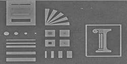
The group was able to produce patterns of tiny dots, 30 nm wide, in patterns of triangles, rectangles and, playfully, an ionic column—the logo of the University of Illinois—at a resolution more precise than nanoimprint lithography. "You end up with a better cut," Fang says. "And we have a stamp that can be reused many times." Fang acknowledges that there are still cost barriers to this glass-etching process: It still requires using a master metallic pattern, made via expensive lithography. However, he points out that only one master pattern, and one glass stamp, is needed to mass-produce an entire line of the same sensor, which may bring large-scale production closer to reality.
SOURCE: MIT; http://web.mit.edu/newsoffice/2011/nano-sensors-glass-1019.html

Gail Overton | Senior Editor (2004-2020)
Gail has more than 30 years of engineering, marketing, product management, and editorial experience in the photonics and optical communications industry. Before joining the staff at Laser Focus World in 2004, she held many product management and product marketing roles in the fiber-optics industry, most notably at Hughes (El Segundo, CA), GTE Labs (Waltham, MA), Corning (Corning, NY), Photon Kinetics (Beaverton, OR), and Newport Corporation (Irvine, CA). During her marketing career, Gail published articles in WDM Solutions and Sensors magazine and traveled internationally to conduct product and sales training. Gail received her BS degree in physics, with an emphasis in optics, from San Diego State University in San Diego, CA in May 1986.
