Near-IR silicon sensor has 20X higher detection efficiency
Tokyo and Fukuoka, Japan--Researchers at the University of Tokyo, Kyushu University, and NMEMS Technology Research Organization have unveiled their approach to improving the sensitivity of silicon (Si)-based near-IR sensors.
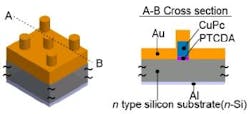
The technology was developed by Isao Shimoyama, a professor at the University of Tokyo; Chihaya Adachi, a professor at Kyushu University; Yoshiharu Ajiki, an exchange researcher at NMEMS Technology Research Organization, and others. They made a device using Si rather than germanium (Ge), improving detection efficiency by adding 10 nm-scale metal nanostructures to Si to increase the electric current generated by collecting near-IR light.
The nanostructures were fabricated using the properties of organic materials rather than more-elaborate methods like photolithography. An organic semiconductor was self-assembled on Si and then a gold (Au) film was deposited on top.
Electric current was efficiently generated for light at a 1.2 μm wavelength. Though the nanostructures were not arranged in a periodic array, their detection efficiency for wavelengths near 1.2 μm was improved by a factor of about 20 over conventional Si detectors.
The announcement was made at IEEE MEMS 2014 (Jan 26 to 30, 2014; San Francisco, CA). The title of the lecture was "Near Infrared Photo-detector Using Self-assembled Formation of Organic Crystalline Nanopillar Arrays."
Source: http://techon.nikkeibp.co.jp/english/NEWS_EN/20140207/332920/

John Wallace | Senior Technical Editor (1998-2022)
John Wallace was with Laser Focus World for nearly 25 years, retiring in late June 2022. He obtained a bachelor's degree in mechanical engineering and physics at Rutgers University and a master's in optical engineering at the University of Rochester. Before becoming an editor, John worked as an engineer at RCA, Exxon, Eastman Kodak, and GCA Corporation.
