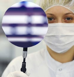
Osram manufacture of gallium nitride LED chips on silicon wafers reaches pilot stage
Sunnyvale, CA--Researchers at Osram Opto Semiconductors have figured out how to manufacture high-performance gallium nitride (GaN)-based blue and white LEDs on 150-mm-diameter silicon (Si) wafers (commonly called “6 inch wafers”). The silicon wafers replace the sapphire substrates commonly used in the industry up to now with no loss of quality, says Osram. Already in the pilot stage, the new LED chips are being tested under practical conditions; the first Osram LEDs on Si could hit the market in as little as two years. (Other similar devices being pursued elsewhere include green LEDs on silicon and blue LEDs on glass substrates, both GaN-based.)
High thermal conductivity, low cost
Silicon is ubiquitous in the semiconductor industry, and thus low in cost compared to sapphire wafers. It has an excellent thermal conductivity of 148 W/(m·K) at 300 K (see http://www.efunda.com/materials/elements/TC_Table.cfm?Element_ID=Si); in comparison the thermal conductivity of sapphire at 300 K is 33 to 35 W/(m·K) depending on the orientation to its crystalline axes (see http://www.almazoptics.com/sapphire.htm).
Osram says that quality and performance data on its fabricated LED Si chips match those of sapphire-based chips: the blue chips in Osram’s standard Golden Dragon Plus package achieve a record brightness of 634 mW at 3.15 V, equivalent to 58% efficiency. These are outstanding values for state-of-the-art 1 mm2 chips driven at 350 mA, according to Osram. In combination with a conventional phosphor converter in a standard housing to form a white LED, these prototypes produce 140 lm at 350 mA with an efficiency of 127 lm/W at a 4500 K color temperature.
“For these LEDs to become widely established in lighting, the component cost must come down significantly while maintaining the same level of quality and performance,” says Peter Stauss, project manager at Osram Opto Semiconductors. “We are developing new methods along the entire technology chain for this purpose, from chip technology to production processes and housing technology.”
It is possible to fabricate more than 17,000 LED chips each 1 mm2 in size on a 6 inch wafer. Larger Si wafers could increase productivity even more; Osram researchers have already demonstrated the first structures on 200 mm Si substrates (“8 inch wafers”).
“Our investments in years of research are paying off, because we have succeeded in optimizing the quality of the gallium nitride layers on the silicon substrates to the point where efficiency and brightness have reached competitive market levels,” says Stauss. “Stress tests we've already conducted demonstrate the high quality and durability of the LEDs, two of our traditional hallmarks.”
About the Author
John Wallace
Senior Technical Editor (1998-2022)
John Wallace was with Laser Focus World for nearly 25 years, retiring in late June 2022. He obtained a bachelor's degree in mechanical engineering and physics at Rutgers University and a master's in optical engineering at the University of Rochester. Before becoming an editor, John worked as an engineer at RCA, Exxon, Eastman Kodak, and GCA Corporation.

