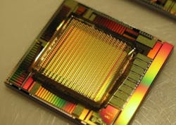
Single-photon avalanche photodiode array chip has onboard signal processing
Duisburg, Germany--The Fraunhofer Institute for Microelectronic Circuits and Systems IMS is a member of a team that has introduced an ultrasensitive CMOS-compatible image sensor based on single-photon avalanche photodiodes (SPADs). The array's pixel structure can count individual photons within a few picoseconds (a thousand times faster than existing versions).
Because each individual photon is taken into consideration, extremely low-light camera images can be captured. The Fraunhofer group developed the device in collaboration with the pan-European (plus Israel) group called Microelectronic Single-Photon 3D Imaging Arrays for low-light high-speed Safety and Security Applications (MiSPIA).
Camera on chip
The new image sensor uses the internal avalanche breakdown effect (a photoelectric amplification effect). To count these events, each of the sensor's pixels includes very precise digital counters. In addition, each sensor chip has its own microlens. And the digital image signals are processed directly on the microchip, eliminating the need for additional analog signal processing.
The Fraunhofer group aims to create a process to produce the same sort of device but with backlit sensors (sensors that receive their light through the wafer).
The Fraunhofer Institute IMS will exhibit the new image sensor at Vision, a trade show for image processing, from November 6 to 8, 2012 in Stuttgart at stand H74 in Hall 1.

John Wallace | Senior Technical Editor (1998-2022)
John Wallace was with Laser Focus World for nearly 25 years, retiring in late June 2022. He obtained a bachelor's degree in mechanical engineering and physics at Rutgers University and a master's in optical engineering at the University of Rochester. Before becoming an editor, John worked as an engineer at RCA, Exxon, Eastman Kodak, and GCA Corporation.
