Cantilever-based nanolithography technique could make cheaper biochips
Raleigh, NC--A new type of dip-pen nanolithography technique that is less expensive than other approaches can be used to create technologies with biomedical applications, say its developers at North Carolina State University (NC State). "Among other things, this type of lithography can be used to manufacture chips for use in biological sensors—biochips—that can identify target molecules, such as proteins or genetic material associated with specific medical conditions," says Albena Ivanisevic, co-author of a paper in Small describing the research. Ivanisevic is an associate professor of materials science and engineering at NC State and associate professor of the joint biomedical engineering program at NC State and the University of North Carolina at Chapel Hill.
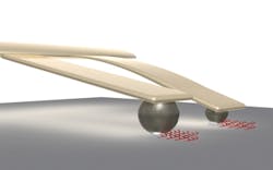
The new technique relies on cantilevers, 150 micron long silicon strips that are tipped with spheres made of polymer or with naturally occurring spores. The spheres and/or spores are coated with ink and dried, and are absorbent enough to soak up water when exposed to increased humidity. Consequently, when the cantilevers are exposed to humidity in a chamber, the spheres/spores absorb water, making the tips of the cantilevers heavier and dragging them down into contact with any chosen surface.
Users can manipulate the size of the spheres and spores and control the patterns created by the cantilevers. For example, at low humidity, a large sphere will absorb more water than a small sphere, and will therefore be dragged down into contact with the substrate surface. The small sphere won’t be lowered into contact with the surface until it is exposed to higher humidity and absorbs more water. Furthermore, the differing characteristics of sphere polymers and spores mean that they absorb different amounts of water when exposed to the same humidity—giving users even more control of the nanolithography.
"This technique is less expensive than other device-driven lithography techniques used for microfabrication because the cantilevers do not rely on electronic components to bring the cantilevers into contact with the substrate surface," Ivanisevic says. "Next steps for this work include using this approach to fabricate lithographic patterns onto tissue for use in tissue regeneration efforts."
The paper was published online August 17 in the journal Small. Lead author of the paper is Dr. Marcus A. Kramer, who did the work at NC State while completing his PhD at Purdue University.
SOURCE: North Carolina State University; http://news.ncsu.edu/releases/wms-ivanisevic-nanolithography/

Gail Overton | Senior Editor (2004-2020)
Gail has more than 30 years of engineering, marketing, product management, and editorial experience in the photonics and optical communications industry. Before joining the staff at Laser Focus World in 2004, she held many product management and product marketing roles in the fiber-optics industry, most notably at Hughes (El Segundo, CA), GTE Labs (Waltham, MA), Corning (Corning, NY), Photon Kinetics (Beaverton, OR), and Newport Corporation (Irvine, CA). During her marketing career, Gail published articles in WDM Solutions and Sensors magazine and traveled internationally to conduct product and sales training. Gail received her BS degree in physics, with an emphasis in optics, from San Diego State University in San Diego, CA in May 1986.
