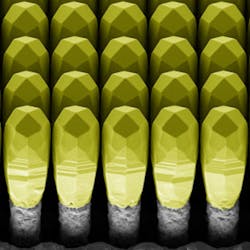
X-ray diffraction reveals 3D mechanics of germanium-crystal arrays
Grenoble, France--Scientists at the European Synchrotron Radiation Facility (ESRF) are using X-ray diffraction to thoroughly understand a new type of nanostructure—square arrays of germanium (Ge) pillars that have very complex geometries and physical attributes.1 The Ge structure has a future in integrated photonics in the form of Ge-based emitters or detectors; the micropillar structure provides a Ge-on-silicon layer that is tougher than a free-standing Ge substrate. The pillars can also be used in high-resolution CMOS X-ray detectors and high-efficiency multijunction solar cells for both space and terrestrial applications.
At ESRF, submicrometer diffraction experiments were used to analyze the tilt and elastic deformation of the pillars after the first micrometer of Ge deposition. Micrometer-scale layers of pure Ge are attractive for IR photodetectors, the final layer of triple-junction solar cells, or as “virtual substrates” for the deposition of GaAs-based layers. Increasing the Ge thickness still further (to several tens of micrometers) would enable the realization of X-ray and particle detectors that are more efficient than their existing Si-based counterparts. The increased efficiency coupled with the good compatibility between Ge and Si leads to the final goal of a pixelated detector in which the Ge absorbs the photons or particles and the resulting signals are handled by Si CMOS readout electronics.
The growth technique of low-energy plasma-enhanced chemical-vapor deposition (LEPECVD) has led to the efficient and fast deposition of such layers, but, once the Ge layer is more than a few micrometers thick, the thermal contraction during the cooling of the substrate back to room temperature after growth causes bending of the substrate and cracking of the Ge layer.
Growth of Ge on Si pillars avoids the problem of bending and cracking on cooling. The Si substrate is patterned into micrometer-scale pillars using standard photolithographic and deep reactive-ion etching techniques. During LEPECVD growth, Ge is deposited mainly on the tops of the silicon pillars due to the directionality of the flux of growth precursors onto the substrate and shadowing from neighboring towers. Surprisingly, the Ge towers expand laterally until the space between them is just a few tens of nanometers, but they never coalesce. Very thick layers (up to 50 micrometers) can be grown, and the whole substrate is almost completely covered with closely-spaced towers. Cracking is completely avoided since each tower is free to elastically accommodate the strain induced by thermal contraction. Each tower could naturally form a single micrometer-sized pixel in a 2D X-ray CMOS camera.
Silicon pillars were studied with only a 1 µm layer thickness of Ge on top, revealing the earliest stage of the growth and the distribution of elastic strain between the Ge and Si. An X-ray beam was focused onto a single tower using a Fresnel zone plate in a wide-angle diffraction geometry to study the spacing and tilt of the crystalline lattice planes, with the diffracted signal collected by a pixelated photon-counting X-ray detector. Full analysis of the synchrotron data is a work in progress and expected to be published shortly.
While only the early stages of Ge growth have so far been studied at the ESRF, future experiments are proposed to study the structural quality of other semiconductors, such as GaAs, grown on Si pillars. GaAs is even more prone to cracking and defective growth when grown on flat Si wafers, but success here holds great promise for many applications in optical and photovoltaic devices such as light-emitting elements directly integrated with silicon electronics or high-efficiency solar cells on light and cheap Si substrates.
Source: http://www.esrf.eu/news/spotlight/spotlight155/index_html/
REFERENCE:
1. C.V. Falub et al., Science 335, 1330 (2012).
About the Author
John Wallace
Senior Technical Editor (1998-2022)
John Wallace was with Laser Focus World for nearly 25 years, retiring in late June 2022. He obtained a bachelor's degree in mechanical engineering and physics at Rutgers University and a master's in optical engineering at the University of Rochester. Before becoming an editor, John worked as an engineer at RCA, Exxon, Eastman Kodak, and GCA Corporation.

