PHOTONICS APPLIED: INTEGRATED PHOTONICS: Can optical integration solve the computational bottleneck?

Truly integrated photonics–the combination of discrete optical components such as light sources, modulators, switches, filters, splitters, waveguides, and detectors on a single integrated platform–remains a “holy grail” in the photonics community. Despite advances by companies like Intel (Santa Clara, CA), an all-optical platform for high-speed communications and signal processing has yet to be realized (see www.laserfocusworld.com/articles/289409).
Companies such as Enablence (Ottawa, ON, Canada), HP Laboratories (Palo Alto, CA), and IBM Research (Yorktown Heights, NY) are working with indium phosphide (InP) and other semiconductor and polymer materials to develop photonic integrated circuits to replace electronic interconnects (see www.laserfocusworld.com/articles/346710). But an ambitious Defense Advanced Research Projects Agency (DARPA) program provides an excellent framework for understanding the challenges that face developers of these next-generation integrated photonics architectures. Funds under the DARPA program, called Ultraperformance Nanophotonic Intrachip Communication Program (UNIC)–pronounced “unique,” were awarded to Sun Microsystems (Santa Clara, CA) and its partners at Kotura (Monterey Park, CA), Luxtera (Carlsbad, CA), the University of California at San Diego (UCSD; La Jolla, CA), and Stanford University (Stanford, CA) to develop optical chip-to-chip and intrachip communications technology that will help meet the challenge of increasing computer performance to keep pace with tomorrow’s computationally intensive applications.
A crisis in computation
The rapid development of applications is fueling the need for more computational power. “Today we are seeing a ‘crisis in computation’ in which the huge data sets being generated by applications in molecular engineering, nuclear power studies, and environmental modeling, for example, are growing faster than the Moore’s Law scaling of available processing power,” says Jack Cunningham, distinguished engineer at Sun Microsystems Physical Sciences Center (San Diego, CA) and coprincipal investigator for UNIC.
In March 2008, DARPA awarded Sun Microsystems $44.3 million to fund the five-year UNIC research project focused on microchip interconnectivity via on-chip optical networks enabled by silicon (Si) photonics and proximity communication. The project aims to interconnect an array of low-cost chips to overcome the fundamental cost and performance limits of scaling up today’s large computer systems.
“We can make faster, better, and cheaper computers by designing better interconnects,” says Ashok Krishnamoorthy, Sun Microsystems Physical Sciences Center distinguished engineer and UNIC principal investigator. “The UNIC project aims to develop optical interconnects that speed the movement of data within chips and between adjacent chips.”
The 2-D macrochip
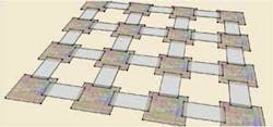
Sun Microsystems’ approach is to drop replaceable memory and processor chips in a tight two-dimensional grid, in which communication between chips takes place optically (see Fig. 1). These “optical-proximity-communication” interconnects offer energy-efficient, near-speed-of-light data transfer on and between chips, whereas traditional on-chip electrical wires are limited to roughly 1/10th the speed of light.1, 2
Optical interconnects also allow additional functionality within this so-called “macrochip” environment: the interconnects can incorporate wavelength-division-multiplexing (WDM) and filter structures that channel particular wavelengths to other parts of the macrochip and perform standard waveguiding and coupling functions. And because the structure is planar in nature, it simplifies heat removal from the chips and power delivery to each chip.
But even before optical connections can be made, an electronic-to-optical (E-O) conversion must take place within the processor and memory chips. Here, the UNIC partners are researching a variety of modulator designs, such as a bank of continuous-wave (CW) laser waveguides interfaced with Si ring resonators that convert the chip’s electronic bit stream to a modulated optical signal. This modulator, and other designs, as well as the key passive and active optical components in the system, are being pursued in parallel tracks by many of the partners. As the project unfolds over its five-year time frame, the technologies will diverge as certain designs prove their viability and manufacturability, says Kannan Raj, Sun Microsystems senior R&D manager on the UNIC project.
Optical-proximity interconnects
Sun Microsystems signed a five-year, $14 million development contract with Kotura specifically for Kotura’s expertise in Si photonics products and its custom Si foundry capabilities. Kotura is actively shipping variable attenuator arrays based on fast carrier absorption in Si p-i-n structures and has experience with interlayer couplers, multichannel multiplexers and demultiplexers, integrated high-speed modulators, and detectors. Its 4200 sq ft fab, which produces complementary-metal-oxide-semiconductor (CMOS)-compatible Class 10 and Class 100 6 in. wafers, is capable of contact and projection photolithography, dry and wet etch, and thin-film and diffusion processes.
“We are excited about being part of such a practical project with solutions that can be commercially viable in five to ten years,” says Mehdi Asghari, CTO at Kotura. Asghari says Kotura’s mirror coupler design–the first step in routing signals from the optical layer that contains the lasers and modulators onto a much larger “reticle size” routing layer for movement between chips–is both polarization and wavelength insensitive, with a proprietary design that makes it low loss (target less than 1 dB) and less sensitive to alignment issues than commercially available mirror couplers. Its diffraction-limited design produces a 0.16 µm2 spot size in Si–important for waveguiding when a single monolithic structure containing, say, an 8 × 8 array of chips, demands ultralow optical loss.
While the total link loss budget for an 8 × 8 macrochip (a combination of 64 total processor and memory chips linked by waveguides and couplers) is approximately 15 dB–no different than a standard telecom link–the initial 2 dB/cm loss budget per transport waveguide must be reduced to fractions of a dB/cm if the project expects to achieve its five-year goal of developing a 10 × 10 macrochip using a 12 in. monolithic coupling structure.
Besides optical loss, the optical-proximity architecture and its associated optical and/or electronic structures must consume a target link energy of 300 fJ/bit with an ultimate goal of 160 fJ/bit for the entire macrochip on all of its wavelengths in the ITU grid–a tall order, considering that commercial Si Mach-Zehnder modulator-based links currently consume around 50 pJ/bit for a single wavelength.
CMOS compatibility
The researchers also plan to take advantage of technology used in nanophotonics. “The beauty of nanophotonics is the use of lithography to fabricate and integrate optical and electronic devices on one chip structure, mimicking the ease of fabricating electronic circuits,” says Yeshaiahu Fainman, Cymer professor of electrical and computer engineering at UCSD, who leads the UNIC effort to develop optical devices on a CMOS-compatible platform such as modulators, detectors, and photonic-crystal WDMs for add/drop wavelength capability.
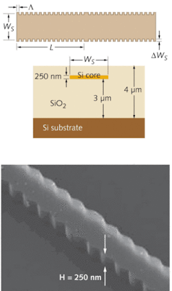
CMOS-compatible isolators (see www.laserfocusworld.com/articles/350662) and routers (see www.laserfocusworld.com/articles/343738 have already been fabricated using optical waveguides and tunable Si microring resonators. Fainman’s “photonic wires” will occupy 1 µm in width, 100 µm in length, and heights of 250 nm compared to many square millimeters for today’s commercially available bulk optical devices.3 These photonic-crystal structures represent a “new physics” for confining light without the associated losses in other optical structures (see Fig. 2).Because Luxtera already has a commercially available CMOS-compatible product–the newly released 40 Gbit/s active optical cable called Blazar–its role in the UNIC project is significant. Built using a standard 0.13 µm silicon-on-insulator (SOI) CMOS manufacturing process, Blazar’s four optical transceivers share a single, inexpensive, unmodulated indium gallium arsenide (InGaAs) CW laser source split into four signals that can be modulated at 10 Gbit/s.4
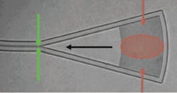
Luxtera is the only company actively integrating optics and electronics on a CMOS platform, according to Thierry Pinguet, principal engineer. “We specifically developed nanophotonic holographic gratings for surface-normal coupling (see Fig. 3),” says Pinguet, “and use a photonics physical-design kit that is modeled after the electronics industries’ design automation tool (for testing current and voltage) that has the ability to test optical wavelength and phase.” Luxtera’s transceivers contain a few hundred optical elements and thousands of transistors. “The UNIC project is the equivalent of hundreds of these transceivers, with 100 to 1000 optical couplings in a square-millimeter area,” says Pinguet.Unfortunately, the 50 pJ/bit Mach-Zehnder modulators currently used by Luxtera fall short of the 300 fJ/bit target. This is where David Miller steps in. Miller is the WM Keck Foundation professor of electrical engineering and codirector of the Stanford Photonics Research Center at Stanford University. He says that the area and power reduction required by the UNIC project demands materials with a stronger electro-optic effect than Si. While much of the project concerns itself with nanoscale confinement of photons, Miller is interested in nanoscale confinement of electrons within quantum wells–a method of modulation that trumps Si Mach-Zehnder modulators by demanding far less energy (up to a factor of 1000 less) and using up less optical real estate (10 mm confinement paths versus 5 mm). Instead of pure Si, he uses multiple very thin layers of germanium (Ge) and Si/Ge.5, 6 And rather than bonding III-V semiconductor devices such as InGaAs to a Si surface, group IV Ge-based quantum-engineered materials with sharper quantum-confined Stark effect can be monolithically integrated using a CMOS process–which is lower in cost and up to two times more energy efficient–that allows devices to be eventually “grown” on the electronic processor and memory chips.
“Intel and others opened the door by showing that silicon is not optically dead,” says Krishnamoorthy. “But we recognize that a pure silicon architecture is a long way from offering the less than 300 fJ/bit communication energy target that we believe is necessary for next-generation computing.” He stresses “manufacturability” as the driving force of the UNIC project. “We aren’t developing a ‘hero’ macrochip here–we are developing over the next five years what we expect will be a commercially viable computing architecture. This is why we’ve partnered with companies like Luxtera and Kotura, which have integrated products on the market today.”
REFERENCES
- A.V. Krishnamoorthy et al., to be published in Proc. SPIE (February 2009).
- J.E. Cunningham et al., IEEE Conf. Proc., 5th IEEE Int’l. Conf. Group IV Photonics 2008, Sorrento, Italy, p. 383 (September 2008).
- H-C Kim, K. Ikeda, and Y. Fainman, J. Lightwave Tech. 25, 5, 1147-1151 (May 2007).
- T. Pinguet et al., IEEE Conf. Proc., 5th IEEE Int’l. Conf. Group IV Photonics 2008, Sorrento, Italy, p. 362 (September 2008).
- R.K. Schaevitz et al., IEEE J. Selected Topics Quant. Elect. 14(4) p. 1082 (July/August 2008).
- J.E. Roth et al., Elect. Lett. 44(1) p. 49 (Jan. 3, 2008).
Why not more chips, bigger chips, or 3-D stacking?
“Gordon Moore said that the number of transistors on a computer chip doubles every two to two-and-a-half years–and this has spurred the historic growth in computer-processing speeds,” says Ron Ho, the second coprincipal investigator on the UNIC project and distinguished engineer at Sun Labs (Menlo Park, CA). “Unfortunately, faster processors don’t solve the communication bottleneck–you still need to move data on and off the chip, which costs physical area and requires energy.” Ho, the circuits expert on the Sun team, explains that this data movement is also the reason that simply adding more chips doesn’t solve the crisis in computation, nor do enormous monolithic chips because yield curves make very big chips disproportionately expensive. Finally, 3-D stacking offers the chance to integrate many chips together at moderate input/output (I/O) expense, but raise equally vexing questions about power delivery, heat removal, and the problem with finding known good die.

Gail Overton | Senior Editor (2004-2020)
Gail has more than 30 years of engineering, marketing, product management, and editorial experience in the photonics and optical communications industry. Before joining the staff at Laser Focus World in 2004, she held many product management and product marketing roles in the fiber-optics industry, most notably at Hughes (El Segundo, CA), GTE Labs (Waltham, MA), Corning (Corning, NY), Photon Kinetics (Beaverton, OR), and Newport Corporation (Irvine, CA). During her marketing career, Gail published articles in WDM Solutions and Sensors magazine and traveled internationally to conduct product and sales training. Gail received her BS degree in physics, with an emphasis in optics, from San Diego State University in San Diego, CA in May 1986.

