TECHNOLOGY REVIEW 2006: The exotic and the everyday spur innovation
Going to a photonics conference to gawk at the technology can be a rewarding experience. There one can see, in the technical sessions, some rather stunning achievements. While no physical laws are violated as leading-edge researchers discover new ways to exploit light in science and engineering, they certainly seem to come close to bending the rules.
Spending time on the exhibit floor can be just as satisfying-that is where one finds the practical results of all this research. In fact, the interaction between research and commercialization is not a one-way street. Anyone who spends time in the technical sessions will discover presentations given by researchers from photonics companies worldwide, both large and small. This technology feeds back to the universities, perhaps through a post-session conversation between interested parties or a later formal collaboration. In addition, the latest and greatest optical instruments seen on the exhibit floor become the building blocks for future research setups.
Sometimes, the results of this research are not found on the exhibit floor of a photonics show. Instead, they find their way into your automobile (advanced lighting, fiber-optic communications), your computer (optical data storage and, someday soon, optical data interconnects), or your pocket (digital-camera sensors, novel lenses for cell phones and cameras). In this way the photonics industry, already many billions of dollars in size, is edging closer to becoming a behemoth the likes of the electronics industry.
Lasers on silicon chips
Bringing practical optical interconnects for computers (board-to-board, chip-to-chip, and perhaps intrachip) and other integrated photonics a step closer to reality, a group of researchers at Intel and the University of California-Santa Barbara (both of Santa Barbara, CA) fabricated electrically injected indium phosphide (InP) 1550-nm-emitting diode lasers on silicon, while researchers at Ghent University (Ghent, Belgium) and the Technical University Eindhoven (Eindhoven, The Netherlands) independently created the same sort of device, but used a different approach (see “Two groups create electrically injected hybrid lasers on silicon”).
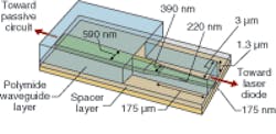
In the Intel version, an InP light source is bonded to a silicon-on-insulator (SOI) waveguide with a mere-nanometers-thick oxide layer serving as the glue via a high-temperature bonding process; the SOI becomes the laser cavity (SOI is an easy-to-create, optically transparent layer well-suited to integrated photonics). In contrast, the Belgian/Dutch device uses benzocyclobutene, a polymer, as the adhesive, with a complete InP laser coupling its light into a layer of SOI via a polymer inverted-taper waveguide (see Fig. 1).
The European group also created similar devices with slightly different geometry that served as photodetectors. Shortening the InP section from the laser’s 500 µm to 50 µm for the detector, the researchers measured a responsivity of 0.23 A/W at 1555 nm.1
In another yield from its continuing push into silicon photonics, Intel has created a high-power monolithic integrated Raman ring-cavity silicon laser that emits up to 30 mW at a 686 nm wavelength.2 Because the laser’s structure can be fabricated entirely by processes akin to conventional computer-chip fabrication (as opposed to the InP hybrid lasers, which must be manipulated into place and then bonded onto SOI), this sort of laser is potentially very low in cost and can be highly integrated with other silicon photonics. The laser is, however, optically pumped (at 1550 nm). Cascading these lasers, each of which lengthens the wavelength of its pump light, can potentially result in a room-temperature mid-IR semiconductor laser.
Invisibility isn’t easy
Research into metamaterials proceeds apace (see “Meta 2006 highlights random, periodic optical metamaterials”), with one result in particular capturing the attention of the popular press: cloaking for invisibility. In the scheme, developed by John Pendry of Imperial College (London, England) and others, a metamaterial structure surrounds an object, redirecting any light striking the metamaterial so that it swerves around the object, then exits the cloak on the other side along its original path, making the object appear not to exist.3
One problem is what the popular press has done with this idea-like describing fanciful devices such as mantles that hide cars or people. In reality, scientists take pains to make sure that a metamaterial is mechanically stable to dimensions much smaller than the relevant wavelength of electromagnetic radiation; this requirement, along with metamaterials’ significant attenuation of light, means that optical-metamaterial-based invisibility cloaks millions of wavelengths in extent (in other words, people-hiders) are impractical.
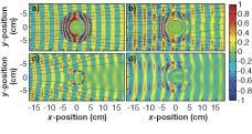
A cloak of invisibility has, however, been demonstrated at microwave frequencies.4 David Schurig and his colleagues at Duke University (Durham, NC), Imperial College (London, England), and SensorMetrix (San Diego, CA) rely on a “transformation-based” cloak design (one in which Maxwell’s equations undergo coordinate transformations) to channel 8.5 GHz (3.6 mm) microwaves around a 50‑mm-diameter copper cylinder. The cylindrical metamaterial structure approximates a 2-D (planar) cloaking device, rather than a full 3-D device; has a lattice spacing of about 3.3 mm, and results in partial invisibility (see Fig. 2). The results are of interest for both civilian (cell-phone transmission) and military stealth use.Microstructured optics of many kinds
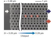
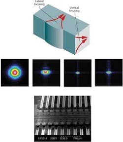
While they once held the position of most exotic laboratory optical material (a spot now occupied by metamaterials, or perhaps surface-plasmon structures), photonic crystals (PCs) have landed solidly in the real world. For example, waveguides within 2‑D PCs can be engineered to slow light down drastically, potentially leading to very compact optical delays and buffers for integrated optics. The bandwidth of such devices, however, is quite narrow. Toshihiko Baba and his group at Yokohama National University (Yokohama, Japan) are refining a variety of techniques to widen the bandwidth (zero-dispersion region) of slow-light photonic-crystal waveguides. In one device, two PC waveguides, one with no holes and the other with small holes offset from the lattice by half a period, are fabricated next to each other. The waveguides have dispersions opposite to one another; as light propagating down one waveguide couples into the other, dispersion is canceled over a 9 nm spectral region and light is slowed to c/50. Baba’s group has also slowed light to from c/30 to c/40 with a 35 nm bandwidth in a chirped-structure PC (see Fig. 3); lower speeds and wider bandwidths will be reached by combining one of these approaches with dynamic tuning (trapping light without compressing the pulses).Many, if not most, typical 2-D and 3-D PCs have only partial bandgaps; achieving a complete bandgap is only possible if the difference in refractive index between the components is high enough. With a refractive index of 2.2 and a large transmission window of 0.45 to 5 mm, lithium niobate (LiNbO3) would seem to be the ideal material for PCs; in addition, its large nonlinear coefficients would allow harmonic generation and other nonlinear effects.
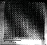
Guangyong Zhou and Min Gu of the Centre for Micro-Photonics and CUDOS (an Australia Research Council Centre of Excellence for ultrahigh-bandwidth devices for optical systems) at Swinburne University of Technology (Hawthorn, Australia) are creating 3-D PCs from LiNbO3 using femtosecond-laser-induced microexplosions to “write” the PC structure. One problem is the strong spherical aberration induced by the large index mismatch between the LiNbO3 and its surrounding medium, which deforms and broadens the focused spot. The researchers sidestep this problem by writing just above the ablation threshold. They have fabricated a 16-layer face-centered-cubic PC that suppresses transmission by up to 30% in its bandgap (see Fig. 4). Further research includes the use of a liquid-crystal phase modulator to sharpen the fabrication beam, which will produce PCs with greater transmission suppression; and studying nonlinear optical effects in the structure.Detecting trace substances
Optical sensing of trace substances is essential in the areas of security, industrial-process monitoring, science, and others. Although such techniques often rely on spectroscopy, other approaches abound. For example, a toroidal optical microcavity developed by Andrea Armani and Kerry Vahala of the California Institute of Technology (Pasadena, CA) sensitively measures the proportion of heavy water (water in which the hydrogen is replaced by deuterium) in a sample of water.5 The ring is immersed in the water sample, and light at a 1300 nm wavelength is coupled into the ring via a tapered optical fiber; the surrounding water slightly absorbs the evanescent light waves at the surface of the ring, affecting the cavity’s Q (quality) factor. The absorption coefficient at 1300 nm for heavy water (0.208 cm‑1) results in a Q of 107; ordinary water (1.374 cm-1) produces a Q of 106.
“The concentration of heavy water that occurs in nature is approximately one in 6400,” says Armani. “Using this technique, it is possible to detect one heavy-water molecule in 10,000. This is the first system that is able to cross the threshold and detect real-time fluctuations in the naturally occurring population.” Armani notes that the most obvious application is in the development of nuclear weapons, because heavy water is typically found wherever someone is trying to control a nuclear chain reaction. However, there are additional applications in water-supply and environmental monitoring.
As for spectroscopic detection of common organic substances (drugs, biological tissue, and industrial chemicals), the mid-IR is all-important, because it encompasses the vibrational modes of many molecules. Harnessing the richness of this spectral region has not been easy, however, due to the lack of an easy-to-use broadly tunable light source. A quantum-cascade laser developed by Daylight Solutions (Poway, CA) and integrated into a package a few centimeters in size has a ±5% tuning range and a center wavelength that can range from 4.5 to 11.0 µm (see “Broadly tunable QC laser enters the market”; also, “Tunable QC laser opens up mid-IR sensing applications”). Combining this laser with a room-temperature mid-IR detector will result in small, rugged optical sensors to detect explosives, pollutants, and even breath-borne substances that indicate disease.
Energy-efficient photonics
Photonic technology contributes to efficient energy use in a variety of ways: non-fossil-fuel energy production (photovoltaics); energy conservation (high-efficiency lighting); and new oil-exploration techniques (see “Photonics and the energy crisis”).
In photovoltaics, cadmium selenide (CdSe) quantum dots assembled in titanium dioxide films form solar cells that are tunable in spectral response (by varying the size of the CdSe dots) and, due to the fact that high-energy photons can produce multiple charge carriers in quantum dots, have the potential for a photon-conversion efficiency of greater than 100% (see “Quantum dots promise next-generation solar cells”). And, in the area of organic photovoltaics, which typically are inefficient and degrade easily, a solar cell based on a new ionic liquid has a 7% efficiency that does not degrade even after 2000 hours of extreme environmental testing (see “Ionic-liquid solar cell boasts 7% efficiency”).
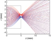
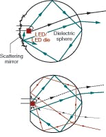
One way to boost the efficiency of an inorganic LED is to find a better way to extract light from the LED chip-which, with its very high refractive index, tends to hold onto much of its light output as a result of total internal reflection (TIR) within the chip. Microstructured, nanostructured, pyramidal, lensed, and other geometries have been devised for this purpose; now, Wanli Chi and Nicholas George of the University of Rochester (Rochester, NY) have created a compact and efficient approach in which an LED is embedded in a transparent sphere with either a planar reflecting cut or a small scattering section (see Fig. 7).6 While most rays from an LED embedded in a dielectric sphere would never escape due to TIR, the scatterer or planar mirror serve to redirect the rays out, with a calculated efficiency of 90% or greater for a refractive index of 1.5. For a 300 µm LED die that emits 40% from its front surface and 15% from each of its four sides, the far-field output approaches a flat-top distribution with a ±10° angular range.Vertical-cavity lasers developed by Novalux (Sunnyvale, CA) can be integrated into a large-screen projection-TV display that consumes a fraction of the electrical power used by a plasma TV (see “Photonics and the energy crisis”); depending on electrical rates, the laser TV would pay for itself through energy savings alone in anywhere from three to eight years. It appears that this technology is going commercial; Novalux is working with Arasor (Mountain View, CA), which provides periodically poled lithium niobate crystals for the TV, in pushing the technology to the market; plans are for consumer-electronics manufacturers Mitsubishi and Samsung to launch projection TVs based on Novalux lasers by December 2007.
Imaging on the edge
The most versatile and productive way to image smaller features (in the sense of seeing, as in a microscope, rather than printing, as in photolithography) is to move to shorter wavelengths. While features as small as 15 nm have been imaged by optical systems that rely on building-size synchrotrons as extreme-ultraviolet (EUV) light sources, few researchers have synchrotrons in their labs. Researchers at Colorado State University (Fort Collins, CO) and Lawrence Berkeley National Laboratory (Berkeley, CA) have imaged 38 nm features with a Fresnel-zone-plate-based optical system combined with a tabletop EUV laser. (Also, see “Coherent light sources reach the extreme ultraviolet.’’)
Joule-level pulses at 5 Hz from a Ti:sapphire laser are focused onto a solid target to produce a plasma in a nickel-like state, producing 13 nm light. A 5-mm-diameter condensor zone plate focuses light onto the object; a 0.1-mm-diameter zone plate with minimum zone size of 50 nm images onto a back-thinned, EUV-sensitive CCD with a 2048 × 2048-pixel array. Elbows, dense lines, and complex test patterns are imaged (see Fig. 8).The industrial-imaging arena has seen much innovation this year. Princeton Lightwave (Cranbury, NJ) has developed a dual-band camera that optically combines two very different optical sensors (see “Infrared cameras vie for multispectral applications”). One sensor, for the visible (400 to 900 nm), is a 2048-element linear CCD array; the other, for IR (1000 to 1700 nm), is a 512-element linear indium gallium arsenide photodiode array. The alignment places each IR pixel at every fourth visible pixel for simultaneous aligned imaging.
In an interesting trend, manufacturers of “smart cameras” (which contain embedded processors and software) are loading up lots of third-party imaging software into their cameras, offering systems integrators multiple software choices when using their cameras (see “Smart cameras look for smarter uses”). For example, a camera by Sony (Tokyo, Japan) can run various x86-based operating systems, allowing the use of either costly but mature imaging software on Windows XP, or free applications being developed for Linux.
Measuring aspheres without null optics
The fabrication of aspheric optics heavily relies on interferometric testing; for surface departures from sphericity of more than a few waves, null optics are usually required (null optics change the interferometer’s spherical wavefront to an aspherical one that matches the desired surface figure of the optic under test). But null optics themselves are difficult to use. Engineers at QED Technologies (Rochester, NY) are extending the capabilities of the company’s subaperture-stitching interferometer (SSI) to handle optics with higher asphericity, simplifying the measurement process.7
The SSI combines a standard interferometer by Zygo (Middlefield, CT) with control software and additional hardware by QED to allow subaperture measurements to be combined into a full-aperture interferogram. When used on an asphere, the SSI measures small, almost spherical segments of the optic and combines them. A mirror fabricated by SSG-Tinsley (Wilmington, MA) for NASA was tested; the 100-mm-diameter ellipsoid had a base radius of -226 mm and an aspheric departure of about 12 µm. Measurements with the SSI agreed well with a separate measurement using null optics (see Fig. 9).Surpassing Blu-ray and HD-DVD?
The newly commercially introduced blue-light-based optical-recording media, Blu-ray and HD-DVD disks, can hold anywhere from 15 to 50 GByte of data; capacities substantially higher than this will require a change in technology. Researchers at the University of Miami (Coral Gables, FL) and New Span Opto-Technology (Miami, FL) may have developed this technology-a holographic optical-storage technique that retains the conventional bit-oriented approach and is thus compatible with existing CD and DVD reading and writing architectures.
Their approach is spectral coding, in which each submicron-size data site on the disk contains many single-bit holograms, all written in the same volume and each written by a different wavelength. The researchers have developed and fabricated a diffractive/refractive lens with a measured depth of focus of 30 µm to write 0.5 µm spots in many colors, and a “wavelength combiner” that takes white light and creates dozens of discrete lines across the visible spectrum, each potentially capable of writing a different wavelength.While the technology is still in an early phase, the researchers have succeeded in writing spectrally coded data with three lasers (red, green, and blue). They have also fabricated a wavelength combiner that spectrally splits white light, spectrally modulates it with a reflective spatial light modulator, and then recombines the light, resulting in many discrete lines (see Fig. 10). In one experiment, six gratings were recorded in one spot. While extending the number of gratings into the dozens (and creating commercially viable hardware) will require further development, the payoff could be quite large.
REFERENCES
1. G. Roelkens et al., Optics Express 14(18) (Sept. 4, 2006).
2. H. Rong at al., Optics Express 14(15) (July 242006).
3. J.B. Pendry et al., Science 312, 5781) (June 23, 2006).
4. D. Schurig et al., Science Express Reports, published online Oct. 19, 2006 [DOI: 10.1126/science.1133628].
5. A.M. Armani and K.J. Vahala, Optics Letters 31(12) (June 15, 2006). (D2O in H2O)
6. W. Chi and N. George, J. Opt. Soc. Am. A 23(9) (September 2006).
7. P. Wu et al., FWI2 session presentation, Frontiers in Optics 2006, the 90th OSA Annual Meeting, Rochester, NY (Oct. 8-12, 2006).

John Wallace | Senior Technical Editor (1998-2022)
John Wallace was with Laser Focus World for nearly 25 years, retiring in late June 2022. He obtained a bachelor's degree in mechanical engineering and physics at Rutgers University and a master's in optical engineering at the University of Rochester. Before becoming an editor, John worked as an engineer at RCA, Exxon, Eastman Kodak, and GCA Corporation.
