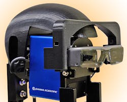
Imaging instrument makes high-resolution measurements of virtual-reality headsets
Virtual reality (VR) and augmented reality (AR) devices are predicted to take the consumer world by storm (at some point), and to help professionals in their work as well. Quantifying the performance of VR and AR devices, however, requires more than, say, a gamer giving the thumbs up or down. A new imaging test system from Gamma Scientific (San Diego, CA) performs high-spatial-resolution color and contrast measurements for near eye-displays (NEDs), such as VR and AR headsets, as well as head-up displays (HUDs). Specifically, the NED Measurement System incorporates compact imaging optics that feed both an integrated camera viewing system and a low-noise, high-accuracy spectroradiometer. An LED spot projector (viewed using the camera) enables the operator to point the optics at a precise position within the display field; selection of the appropriate aperture (using a motorized wheel) then permits measurements over fields of view ranging from 0.1° to 5°.
The system's graphics generator produces test patterns and color fields to measure luminance, color, contrast, uniformity, spectral transmittance, response time (flicker), transmittance modulation-transfer function (MTF) and left/right eye-parallax measurements on subregions of displays as small as a single symbol. The system is intended to aid manufacturers of hNEDs and HUDs for entertainment, medical, avionics, and military applications develop and produce higher-quality and more-consistent products. The system will enable testing to any of the testing standards currently under consideration by the International Committee for Display Metrology (ICDM) committee of the Society for Information Display (SID) and the International Electrotechnical Commission (IEC); these standards are intended to ensure that displays are repeatable and reproducible, and meet a minimum of geometrical and performance criteria. Contact Brock Koren at [email protected].
About the Author
John Wallace
Senior Technical Editor (1998-2022)
John Wallace was with Laser Focus World for nearly 25 years, retiring in late June 2022. He obtained a bachelor's degree in mechanical engineering and physics at Rutgers University and a master's in optical engineering at the University of Rochester. Before becoming an editor, John worked as an engineer at RCA, Exxon, Eastman Kodak, and GCA Corporation.

