Silicon Photonics: Erasable gratings facilitate automated PIC testing
To date, there are a few methods for testing integrated silicon photonics devices and circuits, but they all lack the possibility of comprehensive autonomous testing at the wafer scale. Fabrication of standard grating couplers at input and output locations only facilitates testing of the entire circuit, while use of optical probes is also a problem—these probes are prone to damage when being accessed for testing and can introduce additional loss of individual components or the entire integrated device, thus limiting system lifetime and reliability.
Leveraging earlier work from 2011, researchers at the University of Southampton (Southampton, England) have developed a silicon photonics testing solution by fabricating 'erasable' grating couplers in a silicon-on-insulator (SOI) platform using ion implantation of germanium.1 The gratings allow test access to individual devices on the chip, and are then erased in a laser annealing process that does not impact the optical performance of the photonic circuit.
Fabricating erasable test points
The radiation damage induced in silicon during ion implantation changes the refractive index (amorphous silicon has a refractive index that is approximately 0.5 refractive index units higher than crystalline silicon), allowing the design of optical structures such as grating couplers that can be used as access points for testing other devices integrated on the optical circuit. These test points can then be erased using optical-fiber-based laser annealing.
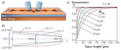
Using germanium (Ge) ion implantation in a CMOS-compatible process, grating couplers were modeled using different grating widths, different numbers of grating lines, and various taper designs (linear, parabolic, and three-stage) and grating lengths to optimize coupling efficiency (see figure). For example, modeling was carried out of standard 500 × 220 nm SOI rib waveguides with 100 nm silicon slab thickness, 120 nm etch depth, 130 nm Ge implantation depth, and various taper designs.
While wider waveguides and a higher number of grating lines improve coupling efficiency, there are obvious tradeoffs between efficiency, compactness, and annealing time. To achieve 5.5 dB coupling loss (including 0.1 dB loss per taper) in a linear taper design with 2 or 10 μm taper widths, for example, requires 5 and 127 μm taper lengths, respectively. All designs were modeled for room-temperature operation at a nominal 1550 nm transmission wavelength.
Annealing is accomplished by using a continuous-wave 488 nm argon (Ar) ion laser to deliver 180 mW power to the amorphous region in a controlled and precise manner. Laser scanning speed is 10 μm/s, making the entire process relatively fast and accurate.
On-wafer measurements
To demonstrate the testing possibilities for a PIC device, erasable gratings were fabricated on SOI wafers using standard CMOS technology, and the grating parameters were optimized. It was found that insertion loss per taper was minimized to 0.1 dB using a 24-μm-long three-stage taper design grating vs. a 55-μm-long linear taper grating (for a grating with 6 μm width and 220 nm depth), and an overall coupling loss of 5.5 dB was achieved. However, there is no fundamental reason why any appropriate figure for the taper loss cannot be chosen for the design process.
Recently, the group also demonstrated an erasable directional coupler using the same technology. The researchers say that this patented (UK 1704690.5) device will also enhance the flexibility of wafer-scale testing systems in the future.
REFERENCE
1. M. M. Milosevic et al., "Towards autonomous testing of photonic integrated circuits," Proc. SPIE, 10108, 1010817 (Feb. 20, 2017); doi:10.1117/12.2251315.
About the Author

Gail Overton
Senior Editor (2004-2020)
Gail has more than 30 years of engineering, marketing, product management, and editorial experience in the photonics and optical communications industry. Before joining the staff at Laser Focus World in 2004, she held many product management and product marketing roles in the fiber-optics industry, most notably at Hughes (El Segundo, CA), GTE Labs (Waltham, MA), Corning (Corning, NY), Photon Kinetics (Beaverton, OR), and Newport Corporation (Irvine, CA). During her marketing career, Gail published articles in WDM Solutions and Sensors magazine and traveled internationally to conduct product and sales training. Gail received her BS degree in physics, with an emphasis in optics, from San Diego State University in San Diego, CA in May 1986.
