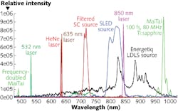
By combining static interferometry and optical-fiber processing, passive interferometer engine (Pie) technology—called the Swiss army knife of optical measurement by its developers at Pie Photonics (Tullamore, Ireland)—measures optical frequency, phase, delay, and amplitude for any narrow or broadband optical light source in a single, static, mobile unit. Using a photonic circuit and a 3648-element camera, Pie-in-a-box captures 500 nm of information with 1 nm resolution in a single click. The resolution is set by the sampling density of the captured interference fringes and number of pixels available—for example, 700 nm light at a sampling density of three pixels per fringe and 3648 pixels across the camera means Pie can achieve an optical-path-delay length of 0.85 mm and a resolution of 0.6 nm.
To produce an interferogram with the Pie engine, individual wavetrains are divided between the arms of a fiber interferometer and then—having traveled similar distances through similar arms—light from respective arms diffracts onto a screen and overlaps. In general, the greater the separation between the exit apertures, the greater the number of interference fringes and the higher the resolution that can be achieved. Pie Photonics has also developed MyPie by interfacing Pie technology with a modified iPhone using a physical photonic-lantern interface (a tapered structure that allows a multimode optical fiber to couple to singlemode components) to demonstrate “smart” mobilization of interferometry. Contact Dominic Murphy at [email protected].

Gail Overton | Senior Editor (2004-2020)
Gail has more than 30 years of engineering, marketing, product management, and editorial experience in the photonics and optical communications industry. Before joining the staff at Laser Focus World in 2004, she held many product management and product marketing roles in the fiber-optics industry, most notably at Hughes (El Segundo, CA), GTE Labs (Waltham, MA), Corning (Corning, NY), Photon Kinetics (Beaverton, OR), and Newport Corporation (Irvine, CA). During her marketing career, Gail published articles in WDM Solutions and Sensors magazine and traveled internationally to conduct product and sales training. Gail received her BS degree in physics, with an emphasis in optics, from San Diego State University in San Diego, CA in May 1986.
