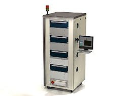
Yelo photonic component characterization system performs in situ optical measurements
This burn-in, life-test, and qualification system provides a modular, temperature-controlled environment for testing multi-chip edge emitters, transceivers, p-i-n photodetectors, avalanche photodiodes (APDs), and transmitter modules. It tests either packaged or chip-on-carrier devices, and can do so with in situ optical measurements.
Yelo Test Systems
Antrim, Northern Ireland
[email protected]
-----
PRESS RELEASE
Yelo announces automated probed laser characterization, lifetest and burn in system for mass production of 40G and 100G active components at Laser World of Photonics Munich
Yelo’s solution reduces testing costs by burning in laser diode bars or photodiode bars at the earliest opportunity, saving the associated costs of rejecting Chip on Carriers and packaged devices.
Yelo’s product and service offering includes:
*Photonic integrated circuit device fixturing
*Controlled temperature accuracy to reduce testing time
*Unique probed Burn In System allowing device sizes down to 1mm²
*Fully automated software
*Thermal management
*LIV Testing in-situ
*Chiller technology to accelerate product throughput
*Mass production, conventional drawer and modular oven systems
Yelo is the market leader in automated laser diode characterization, reliability, lifetest and burn in systems.
For more information contact David Simms, Sales & Marketing Director.
Mob: +44 7714 345 370
Email: [email protected]
-----
Follow us on Twitter
Subscribe now to Laser Focus World magazine; it's free!
