What happens if you etch tellurite glass with a femtosecond laser?
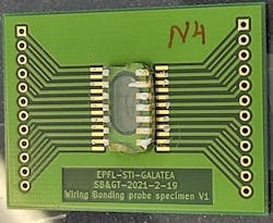
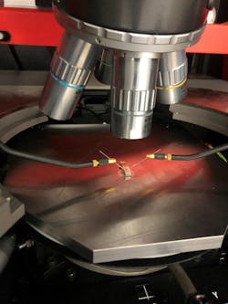
While exploring how atoms within tellurite glass reorganize when exposed to ultrafast pulses of high-energy femtosecond laser light, a team of scientists from Ecole Polytechnique Fédérale de Lausanne (EPFL) in Switzerland and Tokyo Tech in Japan discovered a way to turn tellurite glass into a semiconductor material (see Fig. 1 and video).
This is an amazing discovery because a semiconducting material exposed to daylight can generate electricity—and it holds tremendous potential to turn windows into single-material light-harvesting and sensing devices.
What inspired this work? “Pure serendipity,” says Yves Bellouard, a professor of microengineering, who runs the Galatea Lab at EPFL.
The team’s interest in tellurite glass was “related to a generic question about understanding the underlying mechanism governing self-organization at the nanoscale during laser material processing, including ultrafast crystallization phenomena observed in selected substrates—such as silica, tellurite, sapphire, SiNx, etc.—exposed to femtosecond lasers,” Bellouard says.
As part of her Ph.D. thesis, Gözden Torun, working in the Galatea Lab, was focused on gaining a better understanding of self-organization processes in glass when she made “a serendipitous but brilliant discovery about the formation of a semiconducting tellurium nanocrystalline phase at the glass surface, which then triggered the idea of exploring possible photoconductive properties and our work related to possible light-energy-harvesting devices,” Bellouard says.
Torun made her discovery using tellurite glass, produced by colleagues at Tokyo Tech, and femtosecond lasers to modify the glass and analyze its effects. After etching a simple line pattern on the surface of tellurite glass 1 cm in diameter, she found it could generate a current when exposed to ultraviolet light and the visible spectrum—reliably—for months (see Fig. 2).
Femtosecond laser magic
A femtosecond laser induces localized ionization phenomena, initiated by multiphoton absorption processes, which is further amplified by subsequent cascading events like avalanche and/or tunnel ionizations.
“In short, the inner structure of the material is ‘broken’ and in a state to create conditions to reform material phases that are more stable than their initial metastable—‘glassy’ or not—counterparts,” explains Bellouard. “For tellurite glass, as its structure was being reformed, Torun observed that upon exposure to femtosecond lasers, seeds consisting of clusters of tellurium atoms form and eventually grow into tellurite nanocrystals as the glass phase decomposes.”
It was “the most serendipitous finding,” Bellouard adds, “when she discovered a pure tellurium phase forming—a semiconductive phase embedded within a glass material!”
Rather than using multiple materials to make a device, the team can transform a material locally with a laser so that the transformed region behaves differently than the original material. “The initial material isn’t conductive, nor is it able to harvest photons,” says Bellouard. “But once transformed with a femtosecond laser, it behaves completely differently locally. The key point of using lasers for this work is their ability to localize transformations so that arbitrary patterns can be scribed onto the material to form a device.”
From an economic perspective, not requiring additional materials simplifies processes and is less expensive. And using a laser makes it scalable to any types/sizes of substrates, because it’s simply a matter of scanning a laser beam on the surface.
Further work is still needed to gain a better understanding of the underlying nanocrystallization mechanisms, Bellouard points out, to increase the performance of the device and turn their proof-of-concept exploratory work into an industrial process.
But there are several potential photonics applications that require detecting and quantifying the presence of light at certain wavelengths or spectral ranges, as well as windows capable of harvesting light, that may benefit from the team’s work.
“One big challenge is to ensure modified zones that absorb incoming light are also regions invisible to the naked eyes, so windows keep their function—and let people see clearly through so the glass keeps its aesthetic function,” Bellouard says.
The Galatea Lab explores the transformation of materials under ultrafast lasers—from functional and system integration perspectives. “We explore, in general, the laser-induced formation of crystalline phases in materials, amorphization, or self-organized structures of various types of substrates,” says Bellouard. “One of our key research goals is to generalize these approaches to achieve other types of functions and properties—including electrical, photons processing, or mechanical such as tuning thermomechanical properties.”
The team’s main goal for tellurite now is to improve the process build-up of their preliminary proof of concept.
FURTHER READING
G. Torun, A. Romashkina, T. Kishi, and Y. Bellouard, Phys. Rev. Appl., 21, 014008 (Jan. 5, 2024); doi:10.1103/physrevapplied.21.014008.

Sally Cole Johnson | Editor in Chief
Sally Cole Johnson, Laser Focus World’s editor in chief, is a science and technology journalist who specializes in physics and semiconductors. She wrote for the American Institute of Physics for more than 15 years, complexity for the Santa Fe Institute, and theoretical physics and neuroscience for the Kavli Foundation.

