Ultrafast infrared laser bursts enable writing inside semiconductor chips
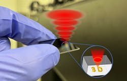
A team of researchers from the French National Center for Scientific Research’s LP3 Laboratory recently developed a method for 3D laser writing anywhere within the three-dimensional space of semiconductor chips made of silicon or gallium arsenide. It’s an enormous advance because it allows the microelectronics industry to finally exploit the entire wafer subsurface of these materials.
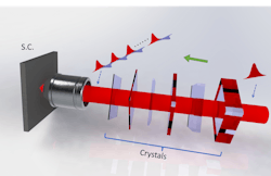
When intense light from ultrafast lasers is focused inside a semiconductor, highly efficient nonlinear ionization along the beam path creates an opaque plasma that prevents it from reaching enough energy localization for material writing. But the team’s method bypasses these strong nonlinear effects with ultrafast bursts of pulses (see Fig. 1).
“The bursts we use have terahertz repetition rates, which means the time between two adjacent pulses is sub-picosecond,” says Andong Wang, a postdoc fellow at LP3 Laboratory.
This timescale is blisteringly short—less than the blink of an eye divided by one billion. Laser energy benefits from this ultrafast burst and can be efficiently accumulated from pulse to pulse until a material modification is initiated. And it allows the researchers to write 3D structures inside various semiconductors.
“Our work is driven by the long-standing challenge of developing 3D laser writing technologies applicable to semiconductor chips,” says David Grojo, the team leader of this work. “It has the potential to move semiconductor manufacturing from a 2D world, imposed by the current use of lithographic planar technologies for fabrication, to high-density 3D integrated devices.”
3D laser writing
As a first target, the team demonstrated the ability to manufacture structures inside semiconductor materials using infrared (IR) ultrafast lasers (semiconductor materials can’t be 3D processed via today’s conventional ultrafast lasers).
“The basis of our research is the important technique of laser direct writing (LDW),” says Wang. “Using this technique, we focus much stronger laser light inside the material to ‘burn’ it. Both the laser and the focusing aspects are carefully engineered so the ‘burn’ process is highly controlled to obtain 3D structures inside the material.”
To do this, they use the standard telecommunication or shortwave-infrared (SWIR) wavelengths for 3D processing inside semiconductors, which penetrates the material so the semiconductors are fully transparent.
As part of the European Horizon project Extreme-Light-Seeded Control of Ultrafast Laser Material Modifications, the team is continuing its previous work to extend the current spectrum of laser processing to a wider range—from UV to IR and even longer wavelengths.
It’s important to note the LDW technique isn’t new and is already widely used to fabricate 3D structures in glass materials. But applying the LDW technique to semiconductors results in very different material responses than glasses.
“It is much more challenging to achieve material writing due to the inherent properties of narrow gap semiconductors, including strongly nonlinear propagation effects, which prevent enough energy localization for permanent modifications of semiconductors,” says Wang.
The researchers say the coolest part of their most recent work is the extremely high repetition rate that helped to solve the nonlinearity problems during laser propagation in semiconductors.Opening doors to new applications
Now that the team has demonstrated the ability to fabricate 3D structures inside semiconductors, it throws the doors wide open to many microelectronics applications.
“We’ve already demonstrated the possibility of writing 3D arrays of modified voxels, from which we could directly derive new optical data storage technologies everywhere inside silicon, the substrate material (platform) in microelectronics chips,” says Grojo. “For shorter-term applications, it may be used for new wafer processing solutions—the way we create defects in a controllable 3D manner, for example, can be used as a very efficient way to dice chips.”
The next step is to “concentrate on the nature of the modifications we achieve and the way we can control their types inside these materials,” says Grojo. “This question is important for refractive index engineering, which is surely an important target given the growing importance of silicon photonics. Laser writing would offer a unique possibility for direct and digital fabrication of 3D architecture monolithic photonics systems inaccessible by current manufacturing technologies. In the future, these new laser modalities may drastically change the way advanced microchips are fabricated.”
FURTHER READING
A. Wang et al., Int. J. Extrem. Manuf., 4, 045001 (2022); doi:10.1088/2631-7990/ac8fc3.

Sally Cole Johnson | Editor in Chief
Sally Cole Johnson, Laser Focus World’s editor in chief, is a science and technology journalist who specializes in physics and semiconductors. She wrote for the American Institute of Physics for more than 15 years, complexity for the Santa Fe Institute, and theoretical physics and neuroscience for the Kavli Foundation.


