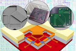
Silicon photonic MEMS designed for compatibility with semiconductor manufacturing
During the COVID-19 pandemic, many of us have become accustomed to working from home offices, accessing cloud data storage, streaming video via broadband, and communicating via video conferencing. What do all of these digital applications have in common? They require an efficient global fiber-optics telecommunications infrastructure (see Fig. 1).
How can we introduce more energy-efficient hardware to meet the future of continuously growing needs for telecom and datacom? This question inspired a group of researchers from École Polytechnique Fédérale de Lausanne (EPFL) in Switzerland, KTH Royal Institute of Technology in Sweden, imec and Ghent University in Belgium, and the University of Sydney in Australia to search for novel and scalable solutions for energy-efficient photonic integrated circuits by merging the previously distinct technologies of silicon photonics and MEMS.
Silicon photonics and MEMS are inherently scalable because they’re both based on standardized semiconductor manufacturing.
“Within this field, photonics is an emerging technology that excels at routing and controlling optical signals on a chip,” says Niels Quack, an associate professor in the University of Sydney’s School of Aerospace, Mechanical, and Mechatronic Engineering, who recently was awarded a 2023 Sydney Research Accelerator prize for this work with photonic MEMS. “And MEMS are already a mature technology that enables extremely precise control of movement at the nanoscale.”
Quack and colleagues built photonic MEMS, small waveguides in silicon, which carry an optical signal that can be precisely moved by integrated electrostatic actuators. This movement can be used to perform different functions, such as modulating the amplitude, phase, direction, or to select channels of spectrum of an optical signal on a chip.
“These operations can be done with very little power consumption,” says Quack. “It’s an enormous improvement of today’s technology, where optical signals on a chip are manipulated using local heaters.”
Silicon photonic MEMS manufacturing
The group’s photonic MEMs (see Fig. 2) are extremely energy efficient, compact, and can now be seamlessly integrated into one of the world’s most advanced standard photonics manufacturing processes at imec.Compatibility with standard platforms is a crucial aspect of this work, because it allows the researchers to leverage the existing ecosystem—including design frameworks, well-characterized high-performance library components, and state-of-the-art photonic manufacturing processes.
The group’s demonstration is an important milestone toward mature, large-scale, reliable photonic circuits with integrated MEMS—showing it’s nearly ready for high-volume production.
“It’s amazing to imagine that we can control the flow of light on a chip by the mechanical movement of a waveguide—only half a micrometer in width—with a precision of a few nanometers,” says Quack.
He points out how mind-bendingly impressive it is to hold a silicon photonic MEMS wafer in your hand, knowing it can host millions of individually movable waveguide devices. “Establishing a reliable wafer-level microfabrication process isn’t an easy task—it took us several years of development, and we achieved it within the framework of the recently completed European Horizon 2020 project MORPHIC.”
As far as challenges go, fabrication tolerances and material compatibilities need to be considered, and microfabrication processes must be carefully dialed in. “Other challenges include the design of novel photonic MEMS components, interfacing of large counts of electrical and optical signals, and to establish control strategies to reconfigure the silicon photonic MEMS-based circuits,” he says.
A wide range of applications can benefit from the group’s advance. “We’ve already demonstrated tunable filters and optical switches for fiber-optic communications,” says Quack. “Further applications include beam-steering for LiDAR 3D sensing that can be used in autonomous vehicles, programming photonic chips that can be reconfigured to perform different functions, or for information processing in quantum photonics.”
What’s next for photonic MEMS?
Quack and colleagues are now pursuing several routes to advance the field of silicon photonic MEMS.
“At the University of Sydney, we conduct research on novel types of MEMS actuators, such as nanomechanical piezo-actuators in silicon photonics,” says Quack. “We expect an important improvement in response time—at least 10 times faster than state-of-the-art components—and a further footprint reduction, which is important for further scaling of the technology.”
In a follow-up to the Horizon Europe research project MORPHIC, a new project called PHORMIC is being led by imec to explore ways to further integrate lasers and amplifiers with silicon photonic MEMS. It targets significant advances in miniaturization and optical signal processing.
Other areas currently being explored include novel photonic MEMS devices or photonic reconfiguration strategies. “These avenues open up new possibilities—think about how MEMS accelerometers, gyroscopes, and microphones are already widely used in consumer electronics,” Quack adds. “Perhaps, someday, there will be a new class of devices in our mobile phones, such as air-quality sensors or micro-3D cameras based on silicon photonic MEMS.”
FURTHER READING
N. Quack et al., Microsyst. Nanoeng. (Mar. 2023); https://doi.org/10.1038/s41378-023-00498-z.
H. Sattari et al., J. Opt. Microsyst., 2 (Nov. 2022); https://doi.org/10.1117/1.jom.2.4.044001.

Sally Cole Johnson | Editor in Chief
Sally Cole Johnson, Laser Focus World’s editor in chief, is a science and technology journalist who specializes in physics and semiconductors. She wrote for the American Institute of Physics for more than 15 years, complexity for the Santa Fe Institute, and theoretical physics and neuroscience for the Kavli Foundation.

