Leaky-wave metasurfaces link free-space optics and integrated photonics
A team of Columbia University (New York, NY) researchers led by Nanfang Yu, an associate professor of applied physics, figured out how to link the realms of free-space optics and integrated photonics.
It’s a big deal because free-space optics and integrated photonics tend to be studied by researchers from different subfields of optics, which has resulted in commercial products that address different siloed needs—such as such as microscopes vs. integrated photonics chips for data and telecom (see video).
“Our work may enable ‘hybrid’ systems that pull from the best of both worlds—free-space optics for shaping the wavefront of light, and integrated photonics for optical data processing—to address many emerging applications such as quantum optics, optogenetics, sensor networks, inter-chip communications, and holographic displays,” says Yu.
Linking free-space optics and integrated photonics
There are two categories of optical systems: one controls light waves propagating in free space, while the other controls light propagating within waveguides on a chip.
Free-space optical systems operate by modulating the optical amplitude, phase, and polarization profiles over the wavefront of light and are indispensable for imaging and display applications. Photonic integrated circuits (PICs), on the other hand, operate upon light confined by and propagating along waveguides to achieve functionalities based on optical information processing, such as computation and sensing.
But linking these two categories of optical systems isn’t easy. “It’s fundamentally difficult to transform a tiny and simple waveguide mode into a broad and complex free-space optical wave, or vice versa,” says Yu.
Demand for hybrid systems made of part PICs and part free-space optics is rising, and many emerging applications can benefit from the best of both worlds, including: a free-space optical link between buildings or between chips that relies on PICs to process information carried by light, while using light waves with shaped wavefronts for robust and high-capacity intercommunication; an optogenetic probe that produces a collimated beam to optically control and monitor neurons located far away from the probe and uses PICs to steer the beam so different neurons can be addressed; and augmented reality (AR) goggles that look and feel as comfortable and fashionable as eyeglasses by combining PICs and free-space optics to reduce system weight and size.
“This motivated us to develop leaky-wave metasurfaces to convert light initially confined in an optical waveguide into an arbitrary optical pattern in free space,” Yu says.
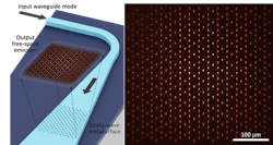
How does the device work (see Fig. 1)? First, a waveguide mode is converted into a slab waveguide mode using a waveguide taper. Then, the waveguide taper is coupled into a leaky-wave metasurface, where it’s decomposed into two orthogonal standing waves that are 90-degrees out of phase.
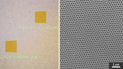
“Our leaky-wave metasurface is made of a nanostructured polymer layer on top of a silicon nitride thin film (see Fig. 2). It’s composed of two sets of meta-atoms designed to convert, respectively, the two standing waves into two surface emissions with independently controllable amplitude and polarization orientation,” Yu says. “The two surface emissions are subsequently merged to form a single free-space wave with completely and independently controllable amplitude, phase, polarization orientation, and polarization ellipticity—all four optical degrees of freedom—at each point over the wavefront.”
Controlling traveling waves within metasurfaces
Yu’s lab previously invented nonlocal metasurfaces that work well converting a standing wave within the metasurface into a free-space wave with controllable phase and polarization state over the wavefront.
The new challenge was to figure out how to control a traveling wave using a metasurface, because light propagates in the form of a traveling wave in PICs.
An a-ha! moment struck when Yu’s team realized that a traveling wave can be decomposed into two orthogonal standing waves with a 90-degree phase difference. “Mathematically, this is simply the Euler’s formula of complex numbers: eix=cos x + i sin x, where eix represents the guided traveling wave, and cos x and sin x the two standing waves,” Yu says. “So we came up with the solution of using two sets of apertures within the metasurface and offsetting them from each other so that one set interacts exclusively with the cosine standing wave and the other exclusively with the sine standing wave.”
Wide range of potential applications for leaky-wave metasurface devices
The team’s device has a wide range of potential applications, including optical displays, optical communications, and quantum optics.
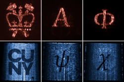
Since their device is thin, transparent, and compatible with PICs, it shows potential for novel optical display systems such as AR goggles and holographic 3D displays (see Fig. 3).
It can also enable chip-to-chip optical communications by providing a compact interface between integrated and free-space optical channels. “An integrated channel on a chip can be connected with another integrated channel on a second chip via a free-space channel established by a transmitting leaky-wave antenna and a receiving leaky-wave antenna,” Yu explains. “Many pairs of such antennas can provide a high-rate and low-loss data link between chips, and leaky-wave transceivers can further use orthogonal spatial modes to carry different channels of information to boost communication capacity.”
Leaky-wave metasurfaces will also be useful for quantum optics, because the team’s device can produce optical lattices to trap cold atoms and molecules. “Compared to traditional methods where optical lattices are produced by interference of multiple beams via free-space optics, our devices can be directly integrated into the vacuum chamber to simplify the optical system, making portable quantum optics applications such as atomic clocks a possibility,” says Yu.
The ability to completely control the four optical degrees of freedom of a wavefront makes the device more advantageous than traditional approaches. Aperiodic and three-dimensional optical trap arrays, for example, can now be created to explore quantum optical phenomena or enable quantum simulations not easily attainable with other platforms.
The team’s current proof-of-principle demonstration is based on polymer and silicon nitride thin films at a near-infrared wavelength. “We plan to demonstrate devices based on silicon nitride, which is more robust, compatible with foundry fabrication protocols, and tolerant to high-optical power operation. We’ll also explore improved designs for high output efficiency and operation in the visible spectrum, which are more suitable for applications such as quantum optics and holographic displays” says Yu.
FURTHER READING
H. Huang et al., Nat. Nanotechnol. (2023); https://doi.org/10.1038/s41565-023-01360-z.
About the Author
Sally Cole Johnson
Editor in Chief
Sally Cole Johnson, Laser Focus World’s editor in chief, is a science and technology journalist who specializes in physics and semiconductors.


