SPECTROMETERS: Chip-based resonant spectroscopy overcomes traditional challenges
STEPHEN J. SWEENEY
Da Vinci's 15th century observation of sunlight diffracting from a prism led to the field that we know today as spectroscopy. From its beginnings as a scientific curiosity, spectroscopy has become a mainstream technique for analyzing matter—ranging from testing the quality of food to estimating the composition of distant objects in our universe. In spite of the wide uptake in the use and exploitation of spectroscopic techniques, there have been relatively few changes in the basic technology. However, an approach that we call "Solo Spectroscopy" offers a key step forward in the field.1-7
Conventional spectroscopy
Spectroscopy in its most common form relies upon diffraction; modern instruments use a diffraction grating rather than a prism to disperse broadband light into its constituent wavelengths. This dispersed light is then collected using either a fixed detector (whereby the grating is rotated) or—in a more common configuration—a fixed grating and a multiple-element charge-coupled device (CCD) detector array. The development of high-dispersion gratings and relatively inexpensive CCDs has led to widespread use of compact, often USB-controlled spectrometers. In such systems, the spectrometer resolution is limited by the dispersion of the grating and the distance from the grating to the detector (the size of the housing).
An alternative approach, known as Fourier-transform infrared (FTIR) spectroscopy, works in a different way: The input light is initially split into two paths with a fraction of the light undergoing a phase shift relative to the other. The light is then recombined, forming a displacement-dependent intensity pattern that is recorded on the detector. The spectrum is then determined by performing a Fourier transform on the data.
Although the FTIR approach is distinct from that of grating-based spectroscopy, there are a number of common features. First, both systems rely on separate dispersion (via a grating or moving mirror) and detection (with a photodetector or array) components. These, along with other optical components such as mirrors or lenses, are then housed in some form of package. Scaled-down versions of these approaches are possible using micro-optoelectromechanical systems (MOEMS) or, for example, by using thin-film or plasmonic filters that provide some means of dispersion.8-10
All these techniques create inherently multicomponent spectroscopy systems that are complex, expensive to manufacture, and potentially suffer from alignment degradation or malfunction, or problems with stray light that ultimately limit spectrometer performance. Overcoming these issues requires a radical change in the way spectroscopy is performed.
Scaling size and performance
Unlike grating or FTIR-based spectroscopy, Solo Spectroscopy uses a single component to undertake both the primary functions of a spectrometer: dispersion and detection. This approach also takes full advantage of semiconductor manufacturing technology to produce a fully functioning spectrometer on an extremely small footprint, more akin to that of a laser diode.
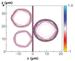
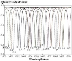
The principle of Solo Spectroscopy is similar to that of optical add-drop multiplexing (OADM) as used for optical switching in wavelength-division multiplexing (WDM) systems.11 In OADM systems, passive devices are used to selectively couple light of a particular wavelength from one optical waveguide to another via some form of selective filter or resonator. Solo Spectroscopy exploits aspects of this approach by coupling broadband light into a waveguide with microdisk or microring resonators closely coupled to the waveguide (see Fig. 1).Because of the large variety of available semiconductor materials, this resonator technology can be implemented over a wide spectral range from the ultraviolet using gallium nitride (GaN) alloys through the near-infrared (NIR) using gallium arsenide (GaAs) or indium phosphide (InP) alloys, and out to the mid-infrared using gallium antimonide (GaSb) alloys or by exploiting intraband transitions in wider-bandgap semiconductors.
By turning the resonator into a p-i-n detector, an electrical signal can be generated that is directly readable using conventional read-out electronics. Therefore, an array of such resonators provides a direct read-out of the spectrum of interest, creating an entirely solid-state miniaturized spectrometer with no moving parts and few of the drawbacks associated with traditional dispersion-based, multicomponent spectrometers.
Concept to prototype
The Solo spectrometer is designed around a customized epitaxial wafer structure that is grown with industry standard metal-organic chemical vapor deposition (MOCVD) or molecular beam epitaxy (MBE) techniques, commonly used to make light-emitting diodes (LEDs) and laser diodes. Judicious structural design means that a waveguide can be built into the structure to effectively guide the incoming light into the eventual spectrometer chip with a thin quantum-well absorbing active region.
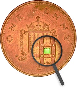
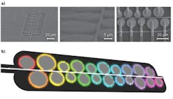
Once grown, the spectrometers are formed on the wafer using a combination of electron-beam and optical lithography techniques that enable precise control of lateral dimensions (sub-10 nm precision) on a wafer-level (wafer diameters of 3–12 in.) scale (see Fig. 3). Several thousand spectrometer chips can be manufactured per wafer, with typical dimensions of 600 µm along each side, 100 µm thickness, and only microgram-level mass values (see photo at top of this page).ZiNIR has fabricated prototype Solo Spectroscopy chips targeting carbon-dioxide (CO2) detection applications in the NIR around 1600 nm. The prototype chips were built on commercially standard InP substrates in a commercial telecommunications device foundry, taking full advantage of mainstream fabrication technology. At the heart of the chip is a 3-nm-thick indium gallium arsenide phosphide (InGaAsP) layer that absorbs light over the wavelength range of interest. This is surrounded by an InGaAsP/InP waveguide structure that efficiently transports the light from the entrance aperture to the resonators.
The first prototypes were designed to test the manufacturability of the resonator and waveguide structures, to optimize the processing technology, and verify electrical operation of the devices; the next prototype phase will focus on the optical and absorption properties of the resonator array.
In addition to the manufacturing advantages, the use of III-V alloys in a monolithic chip ensures long-term reliability consistent with the 20+ year requirement for telecom components, even in hostile or remote environments where servicing and maintenance are difficult or impossible.
The Solo spectrometer chip can be directly integrated into different optical platforms where design features, such as a tapered entrance guide, maximize input coupling from optical fiber or free-space optics. Unwanted light that may otherwise cause stray-light effects is eliminated through control of the semiconductor materials and structured engineering to selectively remove out-of-range wavelengths.
Ubiquitous spectroscopy
The mass-producible nature of the miniature Solo spectrometer chip and its range of wavelength parameters enable new opportunities for spectroscopy. As a single-component-based spectrometer, this resonator approach is well suited to difficult or hard-to-reach environments that are subject to vibration or large changes in temperature that confound traditional spectrometer designs.
Its ultralow mass, scalable and low-cost manufacturing platform, and low power consumption make Solo Spectroscopy amenable to distributed spectrometer networks across ground, airborne, and space platforms, or for medical applications where embedded spectroscopic sensors can work as in vivo medical devices. Distributed networks can be used, for example, to provide global monitoring of pollutant gases with sub-street-level spatial resolution. In addition, the technology offers a hyperspectral imaging capability whereby a single linear array can be used to provide multiple-spectral-window imaging with applications in remote sensing. We believe that Solo Spectroscopy could move spectroscopy beyond its current boundaries and make spectrometers as commonplace as laser diodes or LEDs.
REFERENCES
1. S.J. Sweeney, "Spectrophotometer," Great Britain Patent GB2470115B (2010).
2. S.J. Sweeney, Y. Zhang, and I.D. Goodyer, "The Development of a novel monolithic spectrometer chip concept," Proc. SPIE, 8264, 82640O (2012); http://dx.doi.org/10.1117/12.907118.
3. S.J. Sweeney and Y. Zhang, "Resonator Optimization," EPO Patent Application 11275129.2 (2011).
4. S.J. Sweeney and Y. Zhang, "Suppression of Back Reflection in a Waveguide," EPO Patent Application 11275128.4 (2011).
5. S.J. Sweeney and Y. Zhang, "A Spectrometer," EPO Patent Application 11275127.6 (2011).
6. S.J. Sweeney and Y. Zhang, "Resonator with Reduced Losses," EPO Patent Application 11275126.8, (2011).
7. S.J. Sweeney and Y. Zhang, "Device with Quantum Well Layer," EPO Patent Application 11275125.0 (2011)
8. L.P. Schuler et al., J. Phys. D: Appl. Phys., 42, 13, 133001 (2009).
9. U. Kurokawa, B.I. Choi, and C.C. Chang, Sensors Journal, 11, 7, 1556–1563 (2011).
10. B. Lee and B.I. Choi, "Tunable Plasmonic Filter," US Patent application 2010/0046060.
11. M.A. Popovíc et al., Opt. Lett., 31, 17, 2571–2573 (2006).
Stephen J. Sweeney is CTO at ZiNIR Ltd., Coachmakers Business Centre, 116a Seaside, Eastbourne, East Sussex, BN22 7QP, England; e-mail: [email protected]; www.zinir.com.


