TERAHERTZ SOURCES: Nanoantennas streamline photomixing terahertz source capabilities
HENDRIX TANOTO, JING HUA TENG, and STEFAN A. MAIER
Terahertz sources using photomixing technology are promising for their continuous-wave (CW) emission, wavelength tunability, and compact format thanks to advances in semiconductor laser and photonics integration. However, the lack of efficient room-temperature operation remains a significant technical hurdle in the development of a compact terahertz system. By incorporating nanoantenna structures into a photomixer, a team at A*STAR (Singapore) and Imperial College London (London, England) found that emission power could be enhanced by more than two orders of magnitude compared to a terahertz photomixer using typical interdigitated electrodes. This new nanoantenna-incorporated photomixer could be an enabling technology toward highly efficient, compact CW terahertz sources for high-resolution imaging and spectroscopy systems.
Why photomixing?
Research in far-infrared (IR) electromagnetic waves, which encompasses terahertz waves, effectively started at the beginning of the 20th century, driven by such studies as blackbody radiation.1 In the past two decades, there has been a revival of scientific interest in terahertz waves, fueled by strong public and national interests in tackling security issues of concealed weapons and sophisticated contraband activities, the rising need for ultrawideband communications, and the increasing demand for biomedical imaging and biosciences tools.2
Modern terahertz systems are expected to be compact, efficient, and affordable, making semiconductors the natural materials of choice especially with the backdrop of remarkable developments in integrated circuits and optoelectronics. A pulsed terahertz source based on an Auston switch was one of the first practical semiconductor terahertz sources.3 Pumped by a femtosecond laser with high pulse energy, such sources are able to deliver milliwatt-level peak power and have been widely adopted in terahertz time-domain spectroscopy and imaging systems. These systems are currently addressing niche applications, notably in nondestructive testing in biomedical, pharmaceutical, and food industries.4
Unfortunately, femtosecond-laser-based terahertz time-domain systems lack tunability and tend to be bulky with high cost. It is desirable to have a portable, low-cost, wavelength-tunable, and higher-spectral-resolution terahertz system powered by low-cost, readily available CW semiconductor terahertz sources.
One of the most exciting technologies in semiconductor CW terahertz source development is the quantum-cascade laser (QCL), which uses unipolar carriers and intraband transitions in a repeated stack of semiconductor multiple-quantum-well (MQW) structures instead of interband transitions by electron-hole pairs in a conventional semiconductor laser.5
The emission wavelength of a QCL is determined by tailoring the intraband energy levels of the MQW structures, and is no longer completely dictated by the bandgap energy of the constituent semiconductors. But as the photon energy goes down, especially for operation in the lower terahertz range, the thermal energy of electrons can dominate and cryogenic cooling is essential. Although some new QCL structures—for example, a scattering-assisted design—can operate at 1.8 THz at 163 K, it remains a significant challenge to realize room-temperature operation of QCLs at lower terahertz ranges.6 And while semiconductor electronic devices using resonant-tunneling-diode technology can operate up to 1.1 THz, the achieved maximum emission power is only 100 nW.7
A promising technology to generate CW terahertz radiation at room temperature with decent output power levels and high-resolution tuning is photomixing.8 Advances in semiconductor laser and photonics integration technologies, as well as the recent surge in terahertz metamaterials research, provide many new schemes for the control and manipulation of terahertz waves.9
In our photomixing experimental setup, two tunable lasers with specific terahertz offset frequencies are used as an optical pump (see Fig. 1). The lasers are focused onto the active region of a photomixer to generate carriers in the photoconductive materials. Externally applied electric fields subsequently drive these carriers to the electrode fingers within the active region, generating currents oscillating at terahertz frequencies. This current drives a planar metal antenna that radiates the terahertz waves. In this process, the carrier capture efficiency within the carrier-generation region—the active region—of the photomixer is one of the most crucial factors affecting the power of the radiated terahertz waves.
In a typical state-of-the-art CW terahertz photomixer, the active region consists of interdigitated electrode fingers, originally used in metal-semiconductor-metal photodiodes. To improve the carrier capture efficiency in such an electrode configuration, a tradeoff between electrode finger separation and carrier generation intensity must be made.
Tip-to-tip nanogap electrode structures
The active-region structure that we developed consists of unique nanosized metal electrodes in a tip-to-tip configuration with only a 100 nm gap separating one tip from another, which in essence acts as nanoantenna that enhances the terahertz emission power.10 We fabricated photomixers using low-temperature-grown gallium arsenide (LT GaAs) materials that exhibit suitable characteristics for this purpose: namely, sub-picosecond carrier lifetime, high resistivity, and high carrier mobility.
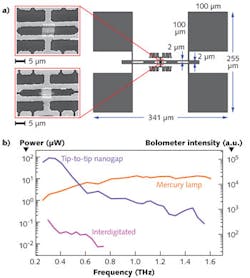
Typical photolithography processing was used to define the microantenna structure and electron-beam lithography was used to define the nanogap electrode active region. This was followed by electron-beam metal deposition and metal lift-off to create the photomixers with interdigitated electrodes and tip-to-tip nanogap electrodes (see Fig. 2).The width and separation of the electrode fingers of the active region are 100 nm and 300 nm, respectively-the same for both interdigitated and tip-to-tip nanogap electrodes. Both devices used a modified Meander terahertz antenna for terahertz radiation and were tested under similar conditions. The terahertz wave emitted from the GaAs substrate side was coupled to a silicon hyper-hemispherical lens and measured via vacuum Fourier-transform infrared spectroscopy (FTIR) with a liquid-helium-cooled silicon bolometer detector.
To approximate the output power of the CW terahertz photomixers, we used a mercury lamp blackbody power-emission source as a reference. The measured CW terahertz emission of the photomixer with interdigitated electrodes and tip-to-tip nanogap electrodes showed significant enhancement in the output power across a bandwidth of approximately 1.3 THz. Within this operating range, the output power of the photomixer with tip-to-tip nanogap electrodes is approximately two orders of magnitude stronger (and emission bandwidth is double) compared to the output power of the photomixer with interdigitated electrodes alone.
Origins of the terahertz power enhancement
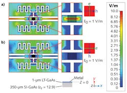
By investigating the electric-field (near-field) distribution of the photomixer under illumination of a 1 THz plane wave using finite-difference time-domain (FDTD) and CST Microwave Studio simulation software from Computer Simulation Technology (CST; Darmstadt, Germany), we observed a greatly enhanced electric-field intensity within the tip-to-tip nanogap active region (see Fig. 3). The dimensions used in the simulations were the same as the fabricated photomixers and the incident terahertz plane-wave strength was kept at 1 V/m for both photomixers.With the electric field of the incident terahertz plane wave aligned along the y-axis, the same direction as the DC bias electric field, the terahertz wave electric field within the tip-to-tip electrodes exhibits approximately 100 times stronger enhanced transmittance as compared to that within the interdigitated electrode structures. The active region of the photomixer is now acting as a nanoantenna. With a more intense electric field at the active region, the electric-field intensity radiated by the terahertz antenna was also enhanced.
Conversely, the photomixer with the interdigitated electrode structure exhibits a much lower electric-field amplitude. The electric field of the incident terahertz plane wave was set along the x-axis, parallel with the dominant direction of the DC bias electric field. Although enhancement is also present in this configuration, the electric field was not radiated but trapped in the substrate instead. As the interdigitated electrode structures resemble parallel-plate capacitors, a larger portion of electromagnetic energy is being stored rather than radiated as compared to the tip-to-tip nanogap electrode structures.
Finally, COMSOL Multiphysics simulation software from COMSOL (Stockholm, Sweden) showed that the capacitance of the tip-to-tip nanogap electrodes is more than one-third smaller than the capacitance of the interdigitated electrodes. The lower capacitance means lower RC time constant, which is beneficial for device operation-especially at higher terahertz frequencies. The significant enhancement of the measured terahertz power originates from the accumulated effects of stronger terahertz antenna radiation and the radiation from the nanoantenna.
REFERENCES
1. E.D. Palik, J. Opt. Soc. Am., 67, 7, 857-865 (1977).
2. M. Tonouchi, Nat. Photon., 1, 97-105 (2007).
3. X.C. Zhang et al., J.Appl. Phys., 71, 326-338 (1992).
4. C. Jansen et al., Appl. Optics, 49, E48 (2010).
5. B.S. Williams, Nat. Photon., 1, 517-525 (2007).
6. S.Kumar et al., Nat. Phys., 7, 166-171 (2011).
7. M. Feiginov et al., Appl. Phys. Lett., 99, 233506 (2011).
8. E.R. Brown et al., Appl. Phys. Lett., 66, 285-287 (1995).
9. H. Tao et al., IEEE J. Select. Topics Quantum Electron., 17, 92-101 (2011).
10. H. Tanoto et al., Nat. Photon., 6, 121-126 (2012).
Hendrix Tanoto is a scientist and Jing Hua Teng is a senior scientist, metamaterials program manager, and deputy head of the Patterning and Fabrication Capability Group at the Institute of Materials Research and Engineering, Agency for Science, Technology and Research (A*STAR) in Singapore; e-mail: [email protected]; www.imre.a-star.edu.sg. Stefan A. Maier is co-director of the Centre for Plasmonics & Metamaterials and professor of Nanophotonics at Imperial College London; www3.imperial.ac.uk.


