Portable spectrometer eases carbon black material characterization

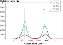
Unlike carbon nanotubes and graphene, carbon black is a form of amorphous carbon used as reinforcement filler in automobile tires and also used in pigments and paint. Its complex material structure limits its analysis to conventional surface area and chemical-absorption tests as well as expensive and time-consuming imaging and x-ray diffraction analysis. Fortunately, carbon materials exhibit strong wavelength-dependent signatures, making Raman spectroscopy favorable for in-line, rapid material characterization on the molecular level. Specifically, a portable Raman spectrometer from B&W Tek can clearly distinguish the G-band in-plane vibrational mode spectra from sp2 hybridized carbon atoms, as well as the D-band or defect band that characterizes the disorder parameters for carbon black.
Using an integration time of 120 seconds and a 40 mW, 532 nm excitation source, the portable i-Raman Plus spectrometer collected data on three different carbon-black samples across a wavelength range including the D-band and G-band with a spectral resolution of 4.5 cm-1. Its back-thinned CCD detector can reach a quantum efficiency up to 90% and thermoelectric cooling reduces dark noise; specifically, the dark noise halves for each 7ºC decrease in device temperature. The BWSpec data analysis software includes baseline correction, peak analysis, and removal of fluorescence-background signals. Reference: D. Yang, “Carbon black at-line characterization using a portable Raman spectrometer,” B&W Tek white paper (Feb. 2015); download at http://solutions.bwtek.com/acton/form/8353/009b:d-0004/0/index.htm.
About the Author

Gail Overton
Senior Editor (2004-2020)
Gail has more than 30 years of engineering, marketing, product management, and editorial experience in the photonics and optical communications industry. Before joining the staff at Laser Focus World in 2004, she held many product management and product marketing roles in the fiber-optics industry, most notably at Hughes (El Segundo, CA), GTE Labs (Waltham, MA), Corning (Corning, NY), Photon Kinetics (Beaverton, OR), and Newport Corporation (Irvine, CA). During her marketing career, Gail published articles in WDM Solutions and Sensors magazine and traveled internationally to conduct product and sales training. Gail received her BS degree in physics, with an emphasis in optics, from San Diego State University in San Diego, CA in May 1986.