TERAHERTZ INSTRUMENTATION: CW terahertz technology overcomes performance and cost concerns

The sheer number of potential applications for terahertz waves (frequencies between 0.1–10 THz) has driven scientists in the past 20 years to develop a variety of terahertz approaches. The most promising applications lie in the fields of sensing, high-bandwidth communication, and, in particular, in terahertz imaging.1
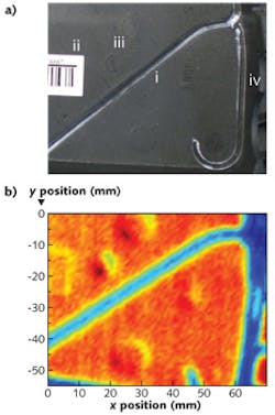
Examples of the latter include the inspection of packages and parcels, quality control of foods or pharmaceuticals, or nondestructive testing of plastic compounds, taking advantage of the ability of terahertz radiation to penetrate many nonmetallic materials.2 For example, Fig. 1 shows images of a polymeric airbag cover: The blackened polymer is opaque for visible light but transparent for terahertz waves. The most relevant feature is a break line with reduced thickness, which is clearly resolved in the terahertz image.3
Today's terahertz instrumentation can be divided into purely electronic sources on one side, and laser-driven (optoelectronic) ones on the other. Optoelectronic devices emit either pulsed or continuous-wave (CW) terahertz radiation. All of these approaches have their merit and have been developed in parallel for many years, depending on the intended field of use.
For example, pulsed optoelectronic terahertz emitters usually provide a high bandwidth (0.1–4 THz). Thus, besides the ability for imaging, these systems enable a spectroscopic analysis of the sample over a broad frequency range. Furthermore, using time-of-flight techniques, pulsed sources can determine the thickness of individual layers within the sample-even on the submillimeter level.
By contrast, optoelectronic CW terahertz systems offer the advantage of frequency selectivity—the source wavelength can be precisely selected and tailored to a specific imaging task. For example, this capability is useful in industrial process control of a gas stream, where the system may be tuned to a relevant absorption line. However, all approaches have had strong impediments, in particular with respect to measurement speed and overall pricing. As a consequence, terahertz imaging has had a hard time finding acceptance.
CW terahertz photomixing
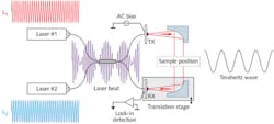
One technique that has reached industrial maturity is an optoelectronic approach known as terahertz photomixing (see Fig. 2).4 Two laser diodes, which are slightly detuned in frequency, generate a beat signal with a frequency in the terahertz range. Via a fiber-optic array, both laser beams are spatially overlapped and the combined signal illuminates the terahertz emitter and terahertz detector.The laser irradiation excites photocarriers in the emitter antenna. An external bias voltage applied to the emitter accelerates the carriers and the resulting photocurrent oscillates at the beat frequency of the two lasers. This gives rise to a new electromagnetic wave—the terahertz wave that is radiated into free space. The terahertz beam may be guided by off-axis-parabolic mirrors, aligned such that the terahertz beam interacts with a sample and is finally focused onto the detector antenna.
The detection process is reciprocal to the generation process. The laser light excites carriers in the detector substrate. Instead of an external voltage, the antenna is biased by the electric field of the terahertz wave. The combination of both generates a photocurrent that is directly proportional to the terahertz electric field. A special feature of this detection scheme is that the terahertz wave is recorded coherently. Thus, both the amplitude and the phase of the signal are recovered, which allows for a more complete analysis of the sample under investigation.
The basic concept of all of this has been around for 20 years, so what has changed over the last few years? In the early days of photomixing, near-infrared lasers were used, whose wavelength had to remain below 870 nm to match the bandgap of gallium arsenide (GaAs)—historically the first material utilized for photomixing. And even though laser technology has come a long way from the bulky Ti:sapphire lasers in the days of yore, today's laser diodes at λ 800 nm still comprise a number of costly, nonstandard optical components.
Telecom laser alternative
A much more compact and inexpensive alternative is telecom-band lasers that operate at an optical wavelength of 1.5 μm. Such lasers are available in highly integrated packages, with miniaturized thermoelectric coolers, optical isolation, and polarization-maintaining fiber pigtails. The linewidth of these distributed feedback (DFB) laser diodes can be as good as 1 MHz. Given sufficiently precise temperature control, an absolute accuracy of the difference frequency of 1 GHz and a resolution of less than 5 MHz can be achieved. Both DFB lasers, together with an additional in-line fiber isolator each, fit into a box 15 × 10 × 5 cm in size.
The flip side of the telecom wavelength range was the lack of suitable terahertz emitters and detectors. An essential prerequisite for photomixers is a short carrier lifetime and a high efficiency of the semiconductor. Unfortunately, the development of fast and efficient photomixers at 1.5 μm has been more difficult than expected. Despite some clever design advances on the emitter side,5 the development of sensitive photoconductive receivers was long regarded as a particular challenge.
One promising receiver material is low temperature (LT) grown indium gallium arsenide (InGaAs), which is known to have the required fast trapping centers. Unfortunately, LT growth of InGaAs increases the dark conductivity by an unacceptable level, rendering the material unsuitable for photomixing. This hurdle has been overcome with newly emerging, InGaAs-based terahertz technology.
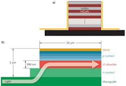
To achieve a fast and highly efficient device, multiple layers of highly photoconductive InGaAs and a material containing deep trapping centers indium (aluminum arsenide, InAlAs) are stacked together (see Fig. 3a). This multilayered sandwich design has a number of advantages. First, the speed of the device—and thus, the usable bandwidth—can be optimized via the thickness of the trapping layer, which is typically as thin as 10 nm. Next, the efficiency can be tuned with the number of layer periods. Typically, about 100 periods are grown to achieve sufficient light absorption.Another improvement is mesa-structuring of the antennae and the use of electrical side contacts as well as removing the photoconductive material at nonilluminated regions. These changes lead to less parasitic dark currents and increase the antenna sensitivity. Consequently, the dynamic range of the detected terahertz signal is significantly higher compared to conventional planar antennas.
As an emitter a standard p-i-n diode is used (see Fig. 3b). The diode comprises a waveguide at the bottom and a bow-tie antenna on top of the device. In such a device, both the efficiency and the bandwidth are optimized, by combining a thin intrinsic absorption layer (300 nm) and a long absorption path (20 μm).
Imaging and spectroscopy
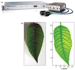
A compact CW terahertz system can include the two-color laser, the controller, and the antenna modules (see Fig 4a). The controller has a field-programmable gate array (FPGA) to precisely tune the wavelength of each laser. It further generates the required bias voltage for the emitter antenna and records the terahertz signal from the detector. The emitter and detector antennas are integrated into fiber-coupled modules, allowing for a flexible use as required by the application.Figure 4b shows a CW terahertz image of a coffee leaf, obtained with a confocal configuration.6 The leaf veins are clearly visible in the terahertz image because of the high absorption effect of water. Terahertz waves can thus be used to identify drought stress in the plant and to optimize irrigation strategies.
A major advantage of optoelectronic over electronic terahertz systems is that, in addition to the ability for imaging, they allow for a spectroscopic analysis of the sample. Thus, sample properties such as the refractive index or absorption coefficient of the leaf can be directly related to the volumetric water content in the leaf.7
REFERENCES
1. W.L. Chan, J. Deibel, and D.M. Mittleman, "Imaging with terahertz radiation," Rep. Prog. Phys., 70, 1325–1379 (2007).
2. C. Jansen et al., "Terahertz imaging: applications and perspectives," Appl. Opt., 49, E48-E57 (2010).
3. M. Scheller, S.F. Dürrschmidt, M. Stecher, and M. Koch, "Terahertz quasi-time-domain spectroscopy imaging," Appl .Opt., 50, 1884–1888 (2011).
4. D. Stanze et al., "Compact cw Terahertz Spectrometer Pumped at 1.5 μm Wavelength," J. Infrared Milli. Terahz. Waves, 32, 225–232 (2011).
5. T. Ishibashi et al., "Uni-traveling-carrier photodiodes," Tech. Dig. Ultrafast Electron. and Optoelectron., 83–87 (1997).
6. M. Salhi, I. Pupeza, and M. Koch, "Confocal Terahertz laser microscope," J. Infrared Milli. Terahz. Waves, 31, 358–366 (2009).
7. C. Jördens, M. Scheller, B. Breitenstein, D. Selmar, and M. Koch, "Evaluation of leaf water status by means of permittivity at terahertz frequencies," J. Biolog. Phys., 35, 3, 255–64 (August 2009).
Nico Vieweg | Director R&D Terahertz, TOPTICA Photonics
Nico Vieweg is Director R&D Terahertz at TOPTICA Photonics (Gräfelfing, Germany).


