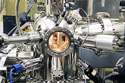
Home-grown ARPES spectroscopy system substitutes for synchrotron light source
Adam Kaminski, an Ames Laboratory (Ames, IA) physicist, developed a new photonics-based technique to study the electronic properties of materials. Two years ago the National Science Foundation closed the synchrotron in Stoughton, WI. More recently, Brookhaven National Lab closed its synchrotron light source to make way for a more advanced and powerful facility. Concerned that this would leave him without the low-energy light source he needed for his studies, Kaminski improvised and developed a new technique that provides a home-grown, laboratory based solution.
RELATED ARTICLE: High-speed x-ray tomography and thermal imaging reveal how lithium-ion batteries explode
Kaminski uses a technique called angle-resolved photoemission spectroscopy (ARPES) in which light energy (photons) directed at a sample being studied cause electrons in the sample to be emitted into a vacuum. An electron analyzer then measures the energy and momentum of these electrons, providing details about the electron properties within the material.
Besides using synchrotron beam lines, lasers can provide the input energy needed, but there were problems with the existing technology. High-energy, tunable lasers offered variable phonon energy, but lacked the resolution necessary for good results. Low-energy lasers provided excellent resolution but the fixed photon energy limited their usefulness.
So Kaminski, who admittedly knew little about lasers, set about finding a way to make a low-energy laser that was tunable. In searching the literature, he found that such a tunable laser had been suggested, but had never been used in ARPES systems. The laser used a potassium beryllium fluoroborate (KBBF) crystal to quadruple the frequency of infrared laser converting photons to the required vacuum ultraviolet (VUV) range.
But Kaminski found that the main source for the KBBF crystals--China--had embargoed their export. However, he found a research group at Clemson University that was able to grow him the crystal he needed. He was also able to obtain funding through the DOE Office of Science to build the new system. As an added bonus, the crystal growth and preparation was commercialized by Advanced Photonic Crystals. This will make them available in the U.S. for applications such as UV photolithography, spectral analysis, and defense.
In simple terms, Kaminski's system uses a pair of lasers, with the first acting as a pump for the second one. The resulting beam consists of very short pulses (one quadrillionth of a second) and very high (400 kW) peak power and is directed into a vacuum chamber that contains lenses, mirrors, and the above mentioned "magic" crystal. This process quadruples the energy of the photons. By tuning the wavelength of the second laser and rotating the crystal, one can then tune the energy of the produced UV photons. The beam is then focused at the sample in an ultrahigh vacuum chamber and a connected electron analyzer measures the electrons emitted from the sample.
"Development of a laboratory-based solution was really important," Kaminski said. "Our beam is smaller, photon flux is higher by one or two orders of magnitude, and energy resolution is better by a factor of 5. Our system has significant advantages," Kaminski said. "It offers much higher resolution. When a researcher has a sample they want tested, we can usually do it the next day." Kaminski has performed ARPES measurements for a number of research groups at Ames Laboratory as well as researchers at Sandia National Laboratory and Princeton. "It's great to have the capability to perform measurements right here in the Lab," he said, "and it's busy 24/7!"
This work was supported by the DOE Office of Science. Ames Laboratory is a U.S. Department of Energy Office of Science national laboratory operated by Iowa State University. Ames Laboratory creates innovative materials, technologies and energy solutions.
SOURCE: Ames Laboratory; https://www.ameslab.gov/news/feature-stories/homegrown-solution-synchrotron-light-source

Gail Overton | Senior Editor (2004-2020)
Gail has more than 30 years of engineering, marketing, product management, and editorial experience in the photonics and optical communications industry. Before joining the staff at Laser Focus World in 2004, she held many product management and product marketing roles in the fiber-optics industry, most notably at Hughes (El Segundo, CA), GTE Labs (Waltham, MA), Corning (Corning, NY), Photon Kinetics (Beaverton, OR), and Newport Corporation (Irvine, CA). During her marketing career, Gail published articles in WDM Solutions and Sensors magazine and traveled internationally to conduct product and sales training. Gail received her BS degree in physics, with an emphasis in optics, from San Diego State University in San Diego, CA in May 1986.
